Sequencing with the MAX16046 System-Management IC
Abstract: Complex devices such as CPUs, ASICs, FPGAs, and memories commonly require power-supply sequencing. The MAX16046 provides a highly integrated solution for sequencing, monitoring, and power-supply margining. This application note presents an example system using multiple devices with specific sequencing requirements, and provides a step-by-step implementation using the MAX16046.
Introduction
Modern electronic devices have complex power requirements involving multiple voltage rails. Power must be supplied for I/O voltages; CPU, ASIC, and FPGA core voltages; PLL voltages; and memory-termination voltages. Other devices need high-voltage, high-current, or low-noise power supplies for applications like radio transceivers, ultrasonic transducers, and LCD or plasma displays.
Designs using multiple power supplies require the designer to pay close attention to power sequencing. Each power-supply rail must be turned on in a specific order to avoid forward-biasing protection diodes within complex multivoltage ICs. If the power supplies are simply turned on simultaneously, the ICs could suffer reliability problems or even latchup.
In addition to power sequencing, some systems implement margining. Voltage margining is a way of controlling the power-supply voltages to fully exercise the corners of all the tolerances and ensure system reliability.
Maxim offers several solutions for power management. This application note focuses on the MAX16046, which sequences, monitors, and margins up to 12 power rails.
Hypothetical Example System
The following hypothetical system will serve as an example throughout the application note. This system is a generic board with a MPC8545 processor and a Virtex? 5 FPGA. Table 1 illustrates the various voltages required by the complex ICs selected for the design.
Table 1. Supply Voltage Requirements
| Name | Description | Spec | Current |
| MPC8548 Voltages | |||
| VDD | Core supply | 1.1V ±55mV | 8A |
| AVDD | PLL supply | 1.1V ±55mV | |
| SVDD | SerDes core supply | 1.1V ±55mV | |
| XVDD | SerDes pad supply | 1.1V ±55mV | |
| GVDD | DDR2 I/O supply | 1.8V ±90mV | 0.5A |
| VTT | DDR2 termination | 0.49 × GVDD to 0.51 × GVDD | 0.5A |
| LVDD | Ethernet supply | 2.5V ±125mV | 0.1A |
| TVDD | Ethernet supply | 2.5V ±125mV | |
| OVDD | I/O supply | 3.3V ±165mV | 0.1A |
| BVDD | Local bus I/O supply | 3.3V ±165mV | |
| Virtex 5 Voltages | |||
| VCCINT | Internal supply | 0.95V to 1.05V | ~10A |
| VCCAUX | Auxiliary supply | 2.375V to 2.625V | 1A |
| VCCO | I/O supply | 1.14V to 3.45V | 1A |
| VDD | ? | 1.8V ±100mV | 2.5A |
| VDDL | ? | 1.8V ±100mV | |
| VDDQ | ? | 1.8V ±100mV | |
The processor and FPGA specify a particular sequencing order to prevent forward biasing the internal ESD diodes for an extended period of time. The sequence order of large multivoltage ICs is generally flexible, but it is best to adhere to the manufacturers' preferred order.
The MPC8548 uses the following sequence order:
- VDD
- AVDD_n, BVDD, LVDD, OVDD, SVDD, TVDD, XVDD
- GVDD
The Virtex 5 uses the following sequence order:
- VCCINT
- VCCAUX
- VCCO
Each device specifies a 50ms maximum power-up time for each power rail. The Virtex 5 also requires that power rails not come up faster than 0.2ms.
The block diagram in Figure 1 efficiently implements the power generation needs of the circuit.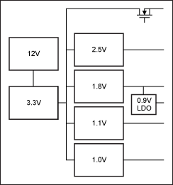
Figure 1. Power block diagram.
Since the 3.3V DC-DC converter provides power to all the downstream point-of-load DC-DC converters, it will need to provide at least 10A at 3.3V. The n-channel MOSFET holds off the 3.3V rail to be used for IO voltages. The 0.9V LDO provides the VTT for the 1.8V DDR2-SDRAM memory.
Now that the sequencing and monitoring requirements for the experimental system have been defined, the MAX16046 can be used to implement them.
Implementing Monitoring, Sequencing, and Margining with the MAX16046
Hardware Configuration
As noted above, the MAX16046 monitors, sequences, and margins up to 12 power supply rails. Monitoring thresholds, the sequence order, margin parameters, and other configuration values are stored in the device's internal EEPROM. Real-time monitoring data can be read over the SMBus? or JTAG interface, which can help check the sequencing order during development.
If a power-supply fault occurs during operation, the MAX16046 can automatically shut down the power supplies and assert configurable fault outputs. The device can also be configured to store information about the failure, including the rail voltages and the channel status, in the internal EEPROM for later analysis. This feature provides a useful tool for analyzing boards that failed in the field, but appear to work properly in the failure lab. Once a fault occurs, the EEPROM is locked so subsequent faults will not overwrite stored fault data.
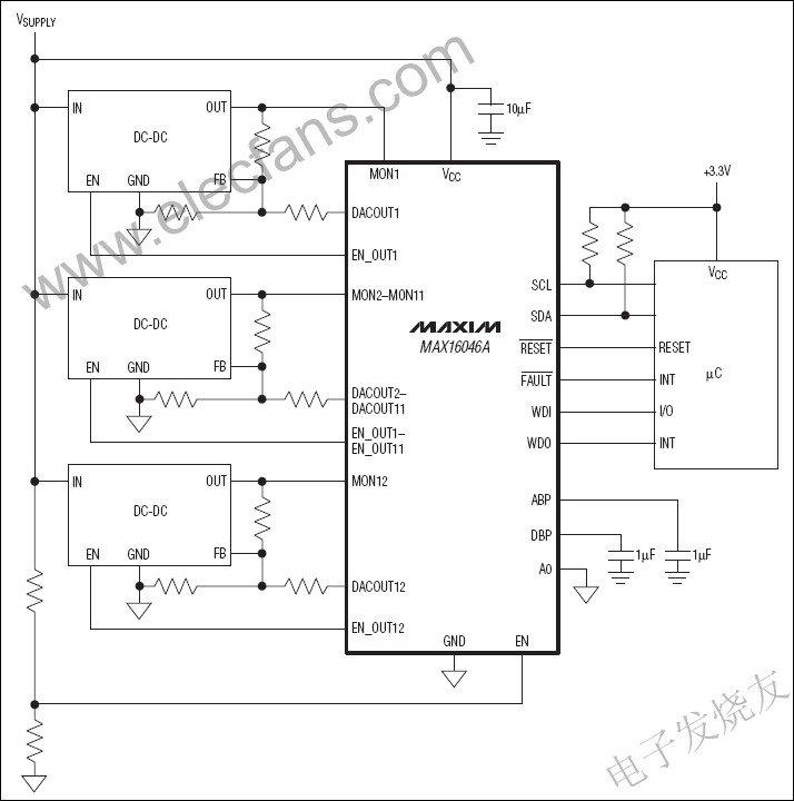
The partial schematic diagram in Figure 2 shows the connections of the MAX16046 in the power architecture shown in Figure 1. The MAX16046 controls the enable inputs of each power supply and monitors the outputs as well. The device also controls the series-pass MOSFET that holds off the 3.3V I/O power rail. The DAC outputs of the MAX16046 are connected to the feedback nodes of several of the power supplies to implement the margining function.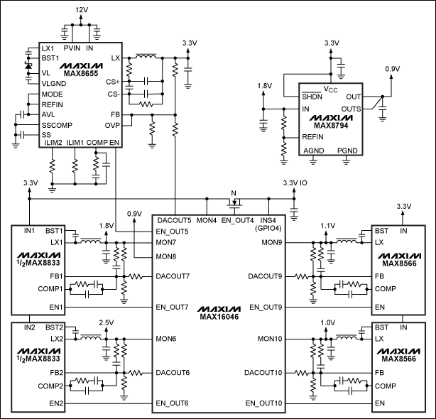
Figure 2. Partial schematic diagram with MAX16046.
Figure 3 shows a more detailed schematic of the circuitry surrounding the MAX16046, including the power connections and in-circuit programming connections. The active-low SYSTEM_RESET signal runs to the reset inputs of the MPC8548 and the Virtex 5. The early-warning signal can warn the MPC8548 to begin a clean shutdown and a soft power-off; the critical fault signal can run to a latch controlling the 3.3V power supply, shutting it off during critical overvoltage events. (FAULT2 is fully programmable, but is set for overvoltage in this application). The watchdog timer input, WDI, connects to the MPC8548 so that the MAX16046 can assert SYSTEM_RESET if the MPC8548 fails to toggle WDI. Active-low MARGINUP# and active-low MARGINDN# run to test points TP1 and TP2 for margining during manufacturing or prototype evaluation.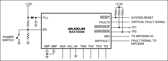
Figure 3. Detailed MAX16046 schematic.
In-circuit programming is accomplished through the JTAG connections, in this example. SDA and SCL run to the MPC8548 so it can query the MAX16046 to obtain fault information or real-time voltage measurements. In-circuit programming is covered in detail in application note 4285, "In-Circuit Programming for the MAX16046–MAX16049 EEPROM-Programmable System Managers."
The MAX16046 will begin sequencing the power supplies when the voltage on EN exceeds 0.525V (typ); it will reverse sequence the supplies when the voltage falls below 0.5V (typ). It is critical that enough bulk capacitance is at the output of the 12V supply to ensure that reverse sequencing completes successfully. The threshold is set at 11.7V to give enough reservoir capacitor voltage for this to happen. Power can also be controlled over SMBus or JTAG for soft power-off applications.
The diode in series with VCC allows the capacitor at VCC to power the MAX16046 during a fault condition. Up to 204ms are needed for the fault-save operation to write the fault data to the nonvolatile EEPROM in the MAX16046. The formula in the MAX16046 data sheet (shown below) yields a minimum capacitor value of 157μF:
Once power-up sequencing has completed, the MAX16046 deasserts SYSTEM_RESET, thereby allowing the processor and FPGA to initialize and begin normal operation.
Software Configuration
The MAX16046 configuration software provides a convenient way of entering configuration parameters without studying register maps or performing endless calculations. Configuring the MAX16046 in our circuit board is accomplished in several steps.
Step 1
Enter the power-supply information into the configuration software setup tab. (See Figure 4.)
More detailed image (PDF, 544kB)
Figure 4. MAX16046 configuration software setup tab with parameters entered.
Each power supply is represented by a row in the spreadsheet-style data table. The 1.8V DDR2 power supply is a dual-output supply, so one "subitem" was added to the row to represent the second monitoring input. Click the row, then click Add Subitem to add the extra monitoring channel for that power supply.
The undervoltage and overvoltage are entered directly as percentages. The software automatically calculates the register values to be loaded into the MAX16046 after clicking Write to Registers.
The margining parameters are entered using the Margining Calculator, shown in Figure 5. The margining calculator will automatically calculate the voltage range, given the reference voltage of the power supply and three resistor values; it will determine the required register values for the margin-up voltage and margin-down voltage.
Figure 5. Margin calculator with parameters for 3.3V rail.
Step 2
Launch the sequencing tab so the sequence order can be determined. Figure 6 shows the sequence order for our circuit. The voltage rails were dragged into the appropriate order by using the mouse cursor. The delay between each rail is set by clicking the underlined blue links at the top row. The delays were set according to Table 2.
Table 2. Slot Delays
| Slot | 0 | 1 | 2 | 3 | 4 | 5 | 6 | 7 | 8 | 9 | 10 | 11 |
| Delay | 12.5ms | 25ms | 25ms | 25ms | 12.5ms | 12.5ms | 20μs | 20μs | 20μs | 20μs | 20μs | 20μs |
More detailed image (PDF, 876kB)
Figure 6. Sequence configuration.
Step 3
Launch the miscellaneous tab to set up the programmable fault outputs, the watchdog timer, and various other parameters. Figure 7 shows the tab for miscellaneous parameters.
More detailed image (PDF, 736kB)
Figure 7. Miscellaneous configuration parameters.
The Any Fault PP configuration for GPIO1 will cause it to assert (push pull) when a sequencing fault occurs or when either the FAULT1 or FAULT2 conditions are true. This signal is sent to the MPC8548 input, which signals that a fault condition has occurred. The MPC8548 can query the MAX16046 through SMBus to determine the cause of the fault.
The Fault 2 PP configuration for GPIO6 will cause it to assert (push pull) when a critical overvoltage fault occurs. GPIO6 can connect to a circuit that cuts power to the board to prevent damage. GPIO6 will assert depending on the check boxes in the FAULT2 column.
GPIO4 is configured for closed-loop tracking (INS4), since that channel is used to hold off the 3.3V IO rail. The power-good threshold of 95% means that this rail goes power good when the voltage on the source of the series-pass MOSFET exceeds 95% of the voltage on the drain.
The reset timeout is set at 200ms. After all power rails reach the power-good state and 200ms has passed, SYSTEM_RESET will go high, releasing the processor and FPGA from reset.
The watchdog timer is configured with a 25.6s initial startup delay after SYSTEM_RESET deasserts. This delay gives the MPC8548 time to complete a boot-up routine before toggling WDI. Dependent means that the initial startup delay is measured from the end of the power-up sequence.
Other Miscellaneous Timers parameters include the Slew-Rate control over the 3.3V IO (400V/s); the 1600ms Auto-Retry delay, which makes the MAX16046 wait for 1.6s after a failed power-up sequence attempt before trying again; and the Fault Up Timer/Fault Down Timer, which allow 25ms for each power rail to come up within the thresholds or fall during reverse sequencing.
Once all the configuration parameters have been set, the data can be saved to a file for mass programming or to be saved into a version control system. The MAX16046 configuration software can generate SVF files for JTAG programming tools.
After loading the configuration file into the assembled target board, the configuration software's monitoring tab can be used to aid with prototype evaluation. The monitoring tab uses the MAX16046's ADC to provide a real-time graph of the rail voltages for each power supply. The sample rate of the graph is too slow to observe the sequence order, but the voltages can be checked.
More detailed image (PDF, 824kB)
Figure 8. Voltage monitoring screen showing sequencing.
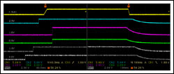
Figure 8 shows a screenshot of voltages in our circuit. Figure 9 shows a composite oscilloscope photo with the voltage rails labeled. The closed-loop tracking slew rate can be observed on the 3.3V IO rail.
More detailed image (PDF, 716kB)
Figure 9. Sequencing scope photo.
The oscilloscope photo can be examined and compared with the sequence order and timing, as configured by the MAX16046 configuration software; it can also be matched with the original sequencing requirements. In this case, the measured sequence order matches the requirements given in the previous section's specification.
Margining can be evaluated by grounding either of the two test points, TP1 and TP2, which causes all the power supplies to rise and fall to the predetermined values. The rail voltage can be measured using the MAX16046 or with a separate voltmeter.
Conclusion
The MAX16046 provides a straightforward method of implementing sequencing, margining, and monitoring in complex, multiple power-supply systems. The MAX16046 configuration software simplifies the configuration of the tolerances and the sequence order.
 電子發(fā)燒友App






評論