Power supplies are perhaps the most crucial elements of a battery-powered system. Knowledge of some basic regulator topologies will help you select or design the right supply configurations for your needs.
Portable computers and digital assistants usually require more than one power supply. These devices may need an AC/DC adapter or battery charger, a high-voltage DC/AC converter for the backlight, and other supplies for lasers, cellular radio transmitters, and auxiliaries. Swapping components in a basic switching-regulator layout alters the circuit topology to create regulators that step up, step down, or invert an input voltage. Substituting a transformer for the inductor produces at least two more regulator circuits or auxiliary output voltages.
The parameters affecting the choice of a switching-regulator topology include the peak currents for the load and the inductor, the voltage level on the power transistors, and the necessity for magnetic and capacitive energy storage. Table 1 shows the seven most common regulator topologies beginning with the simplest (top of table) (which are generally also the most desirable in terms of efficiency, cost, and size) and progressing to more specialized types (bottom). The table also lists the pros and cons of each topology, allowing you to scroll through and find the topology that meets your needs.
Table 1. DC/DC Topology Hierarchy
The table omits complex topologies such as resonant-mode regulators, because their control circuitry consumes too much power for small battery-operated systems. The simpler the circuit, the better: Simple circuits have no magnetics at all or have simple inductors or 1:1 transformers. Off-the-shelf magnetics simplify assembly and minimize costs. Textbooks and magazine articles list other topologies that you can derive from the basic topologies in Table 1. Examples include the Cuk converter, which combines the buck and boost topologies, and the forward converter, which combines a buck converter with half of a push-pull converter.
Switch-mode regulators have two fundamental modes of operation: discontinuous conduction and continuous conduction. Discontinuous conduction lets the inductor current decay to zero during each off period, which causes a transfer of all the stored energy to the output filter during each switching cycle. In the continuous-conduction mode, the inductor current includes a DC component proportional to the load. Operating in the continuous-conduction mode lowers the ratio of peak inductor current to DC-load current, thereby lowering the peak-to-peak ripple current and reducing the core loss.
Dissipation losses occur in the parasitic resistive elements of the regulator circuit. These losses include the series resistance of the battery, the equivalent series resistance (ESR) of the filter capacitors, the on-resistance of the switching element, and the resistances in the conductors, connectors, and wiring. Dissipation losses are proportional to the square of the peak current, so reducing the peak current can greatly minimize these losses. In addition, internal heating degrades a battery's chemistry; thus, excessive peak currents can shorten a battery's life.
The best choice for most battery-powered applications is the buck regulator, provided you can afford the several cells needed to generate a battery voltage higher than the output voltage. Inductor current flows to the load during both phases of the switching cycle, so the average output current equals the average inductor current. In theory, the best efficiency occurs when the input voltage is low, which implies less battery cells in series. Assuming the switch's on-state voltage drop is much smaller than the input voltage, a low input voltage reduces the AC switching losses and the RMS input current.
The boost, or step-up, topologies generate an output voltage that is greater than the input voltage. The boost topologies suit systems with a limited number of battery cells. Because the source voltage and the inductor are in series, the average inductor current equals the DC input current given by:
Inverting and boost topologies operate similarly; however, the inverter's rectified inductor current produces a negative output voltage, which is not aided by the source voltage. The inverting regulator's switching element experiences large voltage swings that impose high switching losses and high stress on the switching transistor. In addition, both the input and output filter capacitors for an inverting or flyback regulator must absorb current waveforms that have large, sharp transitions. Fast-moving waveform edges are absent at the input capacitor of a boost regulator or the output capacitor of a buck regulator.
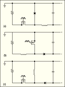
Figure 1. You can invert the input source to create three topologies. The negative buck regulator (a) has an output voltage less than the input. The negative boost regulator (b) has an output more negative than the input. The negative-inverter regulator (c) converts a negative voltage to a positive voltage.
Usually, the best way to design multiple outputs in a battery-powered system is to build several independent supplies. Using simple topologies, you can generate the remaining outputs using off-the-shelf transformers or charge-pump taps.
Coupled-inductor circuits (Figure 2) add an extra flyback winding to the basic buck, boost, and inverting topologies. These hybrid circuits are important, because they combine the advantages of a flyback circuit (isolation and inexpensive multiple outputs) with the benefits of the buck and boost circuits (low peak current and low voltage stress on the switch). The coupled inductor circuit reduces by one the number of windings required by a flyback circuit. This reduction allows the use of an inexpensive 1:1 transformer to generate dual output voltages.
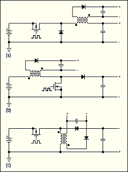
Figure 2. You can create auxiliary outputs by using a flyback transformer instead of an inductor in the basic buck (a), boost (b), and inverter (c) configurations.
The buck regulator with a flyback winding is the superior-performance topology for many battery-powered applications (Figure 3). The configuration has excellent stability, low peak currents, and low output ripple. The output power from the secondary winding depends on the main output's load current and the amount of differential voltage across the primary. Both of these parameters determine the change in core flux that triggers the flyback mechanism.
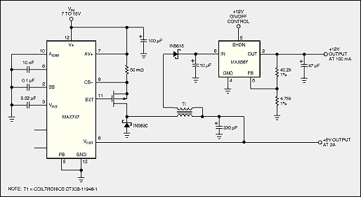
Figure 3. The buck regulator with coupled inductive flyback winding is the best choice for battery-powered systems. The configuration has low peak currents and low ripple in the output voltage.
As a rule of thumb, the total secondary power available is equal to or less than one-half the main output power. This rule applies to only high input voltages. You should reduce the estimate of secondary power for input voltages less than one and one-half times the output voltage. The rule also doesn't apply to circuits containing a synchronous rectifier instead of a simple diode. Synchronous rectifiers have a brief period when the primary current reverses, which causes the circuit to behave as a forward converter instead of a flyback converter. To transfer power efficiently during this forward conduction mode, you must minimize leakage inductance, reduce winding and rectifier impedance, and make the secondary output's filter capacitor as small as the ripple voltage allows.
Diode-capacitor charge pumps offer another inexpensive way to generate multiple output voltages. Any node having repetitive pulses can drive the diode-capacitor network. The gate-driver output or the main switching node of a switching regulator is a good candidate. Boost regulators, for example, can charge a flying capacitor through a grounded diode when the switching node is high (Figure 4a). Turning on the boost transistor forces the switching node and the flying capacitor's positive voltage end to 0V. When the boost transistor turns on, the flying capacitor generates a negative voltage by discharging into the auxiliary output capacitor.
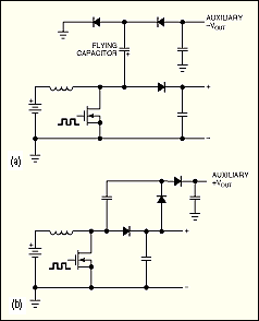
Figure 4. The charge-pump tap offers an inexpensive way to achieve an auxiliary output voltage. Tapping a boost circuit with a flying capacitor (a) creates a negative charge pump. Placing a voltage doubler on the output of a boost circuit (b) creates a high-voltage auxiliary output.
Diode-capacitor charge pumps work best with boost switching regulators, because the switching node swings between a well-defined voltage Vout and ground. Therefore, the line regulation is good. However, the line regulation is not as good when you tap the switching node of a buck or inverting regulator, because the high voltage Vin varies with battery voltage. Load regulation depends mostly on the diode's forward voltage drop. In very low power applications (20mA or less) where an output powers an op amp or an FET-gate driver, you can build the charge pump using an inexpensive 1N4148 diode and a 1mF capacitor.
Portable computers and digital assistants usually require more than one power supply. These devices may need an AC/DC adapter or battery charger, a high-voltage DC/AC converter for the backlight, and other supplies for lasers, cellular radio transmitters, and auxiliaries. Swapping components in a basic switching-regulator layout alters the circuit topology to create regulators that step up, step down, or invert an input voltage. Substituting a transformer for the inductor produces at least two more regulator circuits or auxiliary output voltages.
The parameters affecting the choice of a switching-regulator topology include the peak currents for the load and the inductor, the voltage level on the power transistors, and the necessity for magnetic and capacitive energy storage. Table 1 shows the seven most common regulator topologies beginning with the simplest (top of table) (which are generally also the most desirable in terms of efficiency, cost, and size) and progressing to more specialized types (bottom). The table also lists the pros and cons of each topology, allowing you to scroll through and find the topology that meets your needs.
Table 1. DC/DC Topology Hierarchy
| ? |
|
|
 |
Inexpensive Very small Low quiescent current Low noise/EMI |
Inefficient at high input voltages |
 |
Inexpensive Very small Can boost or invert |
Limited range of input/output voltage ratio |
 |
Lowest peak current Only one switch voltage drop Low-ripple current in output-filter capacitor Simple inductor Low switch-stress voltage |
High-side switch |
 |
Low peak current Low-side switch Simple inductor Low switch-stress voltage |
Output can't be completely turned off No short-circuit protection |
 |
Simple inductor |
High-side switch High peak currents |
 |
Isolated output Multiple outputs Steps up/down, inverts Low-side switch |
High peak currents High switch-stress voltage |
 |
Isolated output Multiple outputs Steps up/down, inverts Core doesn't need to store energy Easy to filter |
Two switches required Two rectifiers required |
The table omits complex topologies such as resonant-mode regulators, because their control circuitry consumes too much power for small battery-operated systems. The simpler the circuit, the better: Simple circuits have no magnetics at all or have simple inductors or 1:1 transformers. Off-the-shelf magnetics simplify assembly and minimize costs. Textbooks and magazine articles list other topologies that you can derive from the basic topologies in Table 1. Examples include the Cuk converter, which combines the buck and boost topologies, and the forward converter, which combines a buck converter with half of a push-pull converter.
Switch-mode regulators have two fundamental modes of operation: discontinuous conduction and continuous conduction. Discontinuous conduction lets the inductor current decay to zero during each off period, which causes a transfer of all the stored energy to the output filter during each switching cycle. In the continuous-conduction mode, the inductor current includes a DC component proportional to the load. Operating in the continuous-conduction mode lowers the ratio of peak inductor current to DC-load current, thereby lowering the peak-to-peak ripple current and reducing the core loss.
Peak Current Is Critical
In battery-powered converters, the peak inductor current is important, because it affects the battery life and parasitic losses. The peak currents depend partly on the average load current, which varies with the regulator topology. The reference (at the end of this article) presents equations for the peak-versus-load current associated with three regulator topologies. Peak inductor current also depends on the control circuit and whether the inductor current is continuous. The voltage stress on the switching transistor is usually not an issue in battery-powered converters. The 20V and 50V breakdown voltage ratings for standard logic-level MOSFETs are adequate for the low input and output voltages found in battery-powered systems.Dissipation losses occur in the parasitic resistive elements of the regulator circuit. These losses include the series resistance of the battery, the equivalent series resistance (ESR) of the filter capacitors, the on-resistance of the switching element, and the resistances in the conductors, connectors, and wiring. Dissipation losses are proportional to the square of the peak current, so reducing the peak current can greatly minimize these losses. In addition, internal heating degrades a battery's chemistry; thus, excessive peak currents can shorten a battery's life.
The best choice for most battery-powered applications is the buck regulator, provided you can afford the several cells needed to generate a battery voltage higher than the output voltage. Inductor current flows to the load during both phases of the switching cycle, so the average output current equals the average inductor current. In theory, the best efficiency occurs when the input voltage is low, which implies less battery cells in series. Assuming the switch's on-state voltage drop is much smaller than the input voltage, a low input voltage reduces the AC switching losses and the RMS input current.
The boost, or step-up, topologies generate an output voltage that is greater than the input voltage. The boost topologies suit systems with a limited number of battery cells. Because the source voltage and the inductor are in series, the average inductor current equals the DC input current given by:
I = Pin/Vin.Sometimes called the buck-boost circuit, the inverter topology generates an output voltage that has opposite polarity from the input voltage. Inverting and flyback regulators are electrically equivalent when considering peak currents and voltage stress. These topologies are most suitable to applications that require negative or galvanically isolated outputs. In general, however, the high peak currents make inverting and flyback topologies the least attractive of the simple regulators.
Inverting and boost topologies operate similarly; however, the inverter's rectified inductor current produces a negative output voltage, which is not aided by the source voltage. The inverting regulator's switching element experiences large voltage swings that impose high switching losses and high stress on the switching transistor. In addition, both the input and output filter capacitors for an inverting or flyback regulator must absorb current waveforms that have large, sharp transitions. Fast-moving waveform edges are absent at the input capacitor of a boost regulator or the output capacitor of a buck regulator.
Upside-Down Topologies Have Low-Side Switch
You can implement three negative topologies by connecting the classic buck, boost, and inverting topologies upside down. Because the input source is inverted, you must reverse the polarities for the switch and the rectifier (Figure 1). Although there are no ICs currently available for the negative topologies, you can use a positive-output IC. Negative buck regulators enjoy all the advantages of positive buck regulators and have the added benefit of a low-side switch. The low-side switch arrangement allows the use of a low Ron n-channel MOSFET with simple drive requirements. The negative buck regulator has some appeal as an alternative for the main positive regulator, provided the battery can float with respect to system ground. If battery floating is possible, you can refer ground to the negative output and the battery's positive terminal to Vout.
Figure 1. You can invert the input source to create three topologies. The negative buck regulator (a) has an output voltage less than the input. The negative boost regulator (b) has an output more negative than the input. The negative-inverter regulator (c) converts a negative voltage to a positive voltage.
Usually, the best way to design multiple outputs in a battery-powered system is to build several independent supplies. Using simple topologies, you can generate the remaining outputs using off-the-shelf transformers or charge-pump taps.
Coupled-inductor circuits (Figure 2) add an extra flyback winding to the basic buck, boost, and inverting topologies. These hybrid circuits are important, because they combine the advantages of a flyback circuit (isolation and inexpensive multiple outputs) with the benefits of the buck and boost circuits (low peak current and low voltage stress on the switch). The coupled inductor circuit reduces by one the number of windings required by a flyback circuit. This reduction allows the use of an inexpensive 1:1 transformer to generate dual output voltages.

Figure 2. You can create auxiliary outputs by using a flyback transformer instead of an inductor in the basic buck (a), boost (b), and inverter (c) configurations.
The buck regulator with a flyback winding is the superior-performance topology for many battery-powered applications (Figure 3). The configuration has excellent stability, low peak currents, and low output ripple. The output power from the secondary winding depends on the main output's load current and the amount of differential voltage across the primary. Both of these parameters determine the change in core flux that triggers the flyback mechanism.

Figure 3. The buck regulator with coupled inductive flyback winding is the best choice for battery-powered systems. The configuration has low peak currents and low ripple in the output voltage.
As a rule of thumb, the total secondary power available is equal to or less than one-half the main output power. This rule applies to only high input voltages. You should reduce the estimate of secondary power for input voltages less than one and one-half times the output voltage. The rule also doesn't apply to circuits containing a synchronous rectifier instead of a simple diode. Synchronous rectifiers have a brief period when the primary current reverses, which causes the circuit to behave as a forward converter instead of a flyback converter. To transfer power efficiently during this forward conduction mode, you must minimize leakage inductance, reduce winding and rectifier impedance, and make the secondary output's filter capacitor as small as the ripple voltage allows.
Diode-capacitor charge pumps offer another inexpensive way to generate multiple output voltages. Any node having repetitive pulses can drive the diode-capacitor network. The gate-driver output or the main switching node of a switching regulator is a good candidate. Boost regulators, for example, can charge a flying capacitor through a grounded diode when the switching node is high (Figure 4a). Turning on the boost transistor forces the switching node and the flying capacitor's positive voltage end to 0V. When the boost transistor turns on, the flying capacitor generates a negative voltage by discharging into the auxiliary output capacitor.

Figure 4. The charge-pump tap offers an inexpensive way to achieve an auxiliary output voltage. Tapping a boost circuit with a flying capacitor (a) creates a negative charge pump. Placing a voltage doubler on the output of a boost circuit (b) creates a high-voltage auxiliary output.
Diode-capacitor charge pumps work best with boost switching regulators, because the switching node swings between a well-defined voltage Vout and ground. Therefore, the line regulation is good. However, the line regulation is not as good when you tap the switching node of a buck or inverting regulator, because the high voltage Vin varies with battery voltage. Load regulation depends mostly on the diode's forward voltage drop. In very low power applications (20mA or less) where an output powers an op amp or an FET-gate driver, you can build the charge pump using an inexpensive 1N4148 diode and a 1mF capacitor.
 電子發(fā)燒友App









評論