This article describes the use of a MAX5003 controller in designing a power supply with -48V input and +5V/1A output. It demonstrates that such power supplies can be designed with small form factors and at lower cost while optimizing their design for best performance.
These high-input-voltage power supplies are found in PABX gear and telecommunication applications (base stations and central offices) as well as data communication applications such as switches, routers, and hubs. Typically, a high-power (-48V) backplane power supply feeds various line cards in a rack-mounted cabinet. Each card converts -48V to an isolated supply voltage and also generates other supply voltages as required on the secondary side of the isolation transformer.
Such schemes make the line cards modular, allowing you to expand a system by adding more line cards instead of redesigning the main power-supply bus. Likewise, you can replace a defective board without affecting system performance. Isolated power supplies prevent noise coupling between the line-card outputs, and they also prevent a single shorted line-card output from causing catastrophic failure in the system.
Although backplane voltages are nominally -48V, the power supplies designed for that environment should operate with inputs as low as -36V and as high as -72V and tolerate transients as high as -100V. As you add more cards to a rack-mounted cabinet without increasing its size, the closer spacing between cards necessitates the use of lower profile components on each board. Similarly, the greater functionality of line cards such as xDSL compels designers to squeeze the power-supply circuitry into less PCB real estate. Greater packing density also raises thermal-management issues.
Many line cards are on standby 90% of the time, so to keep light-load efficiency high, a power supply should have low quiescent current in the standby mode as well as high efficiency at full load. Powering the PWM controller from a high-input-voltage supply makes light-load efficiency difficult. A good source of low voltage is available after the supply is running (the output), but only the high voltage is available during startup.
Many PWM controllers use an external bleeder resistor and capacitor for startup. After the external capacitor charges to a preset undervoltage lockout voltage, the PWM controller begins operating, taking its power from a low voltage derived from an auxiliary winding in the transformer. No provision is made to turn off the bleed resistor, so it continues to waste power during normal operation. A larger resistor value conserves power but lengthens the power supply's startup time.
An alternative solution replaces the resistor-capacitor combination with a zener diode and current-limiting resistor. This approach solves the startup problem, but the bleed current remains, serving no purpose after startup but to heat up the power resistor. The MAX5003 includes a high-voltage startup FET transistor and preregulator (Figure 1), which restricts the quiescent power dissipation during normal operation by disconnecting the high voltage after startup. The IC withstands input voltages as high as 110V, and an external resistor divider at the input helps program the system's undervoltage lockout (UVLO) voltage.
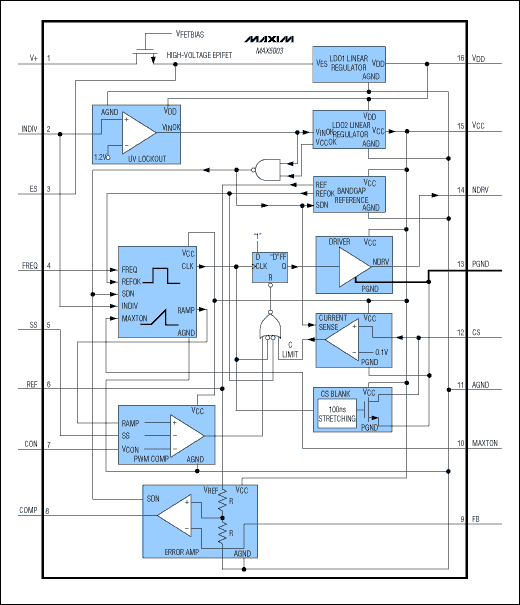
Figure 1. This functional diagram of the MAX5003 PWM controller contains all the functions necessary for designing cost-effective flyback and forward-mode DC-DC converters.
At power-up, the internal FET transistor is biased on, providing power to an internal low-dropout linear regulator (LDO1). In turn, LDO1 powers the linear regulator LDO2, generating a VCC supply for the device. Once the input voltage exceeds the preset UVLO threshold, the internal high-voltage FET transistor turns off, disconnecting high voltage from the device. Power for the MAX5003 now derives from an auxiliary winding connected to the VDD pin. Biasing the VDD pin between 10.75V and 18.75V disables LDO1, allowing LDO2 to bias the device by generating a regulated VCC supply voltage.
Because its high-voltage input is disconnected after power-up, the MAX5003 draws only leakage current (μA) from the high-voltage supply. With a typical supply current (2mA) and VDD bias voltage (12V), the MAX5003 quiescent power dissipation in normal operation is only 24mW (vs. 200mW if the current were drawn from a 100V source). The MAX5003 is designed to operate from input voltages in the 25V to 110V range (connected to its V+ pin). For lower voltage operation, bypass the internal high-voltage FET by connecting the V+ and ES pins together and leaving the VDD pin unconnected. In this case, the external supply voltage at the V+ and ES pins is limited to an 11V to 36V range.
The MAX5003 is a very flexible PWM voltage-mode controller. It can operate in continuous- or discontinuous-current modes and in the flyback or forward-converter topology. Flyback is a versatile, low-cost topology that allows multiple outputs, input-to-output isolation, and simple design. The MAX5003 with flyback topology is recommended for low- to medium-power applications (under 20W). At higher output power levels, the flyback topology becomes less desirable because large peak currents can develop in the external switch transistor and rectifying diode. This action can cause high ripple (especially in discontinuous-current mode) that requires a large and expensive output capacitor. Finally, the flyback-converter stability can be problematic, especially in continuous-mode operation.
For these reasons, the forward-mode topology is recommended for use with the MAX5003 at higher power levels (20W to 50W). Forward mode allows higher power capability than the flyback topology, and it also produces lower ripple due to its output LC filter and lower peak-to-average current ratios. Trade-offs (vs. the use of a flyback topology) include a more complex magnetics design, a higher component count, and an external switch with a voltage rating twice the input voltage (due to the use of an extra clamp-reset winding). When compared with earlier generation devices, the MAX5003 offers features with better customer benefits (Table 1).
Table 1. Selected MAX5003 features
|
|
|
| Input voltage range 11V to 110V | Direct high-voltage operation |
| Voltage-mode control with current limiting | Easy compensation, good input-transient response, and good noise immunity |
| High-voltage startup circuit with shutoff | High efficiency even at light loads, and a low thermal profile for the system |
| Programmable switch-current limit | Flexibility and lower cost FETs |
| Adjustable frequency to 300kHz and external-frequency synchronization | Flexibility, reduced EMI, smaller magnetics, and smaller overall designs |
| Adjustable soft-start and undervoltage lockout | Flexibility, reliability, and simpler bus-distribution design |
| Input feed-forward | Fast line-transient response |
| Precision internal reference, ±2.5% over temperature | Voltage accuracy and stability |
| Modern 16-pin QSOP package | 43% smaller footprint than comparable ICs in 14-pin SO packages |
Design example: +48V to +5V/1A flyback supply
This section describes the design of a flyback power supply using the MAX5003, resulting in a very compact, low-cost and efficient circuit (Figure 2). (For greater detail on the design steps, see the MAX5003 data sheet.) This design has a nonisolated output for the sake of simplicity and straightforward description. Maxim offers a power supply with similar specifications and an isolated output, already assembled and tested for easy evaluation (MAX5003EVKIT) (Figure 3). Briefly, the design methodology for Figure 2 is as follows:- Determine the requirements: VIN, VOUT, IOUT, ripple, and settling time.
- In free-running mode, choose the programming resistor for the FREQ pin. In synchronized mode, choose the external fCLK frequency.
- Determine the transformer turns ratio, and check the maximum duty cycle.
- Determine the transformer primary inductance.
- Complete the transformer specifications by listing the primary maximum current, the secondary maximum current, and the minimum duty cycle at full power.
- Choose the programming resistor for the MAXTON pin.
- Choose a filter capacitor.
- Determine the compensation network.
- Requirements: 36V < VIN < 72V, VOUT = 5V, IOUT = 1A, ripple <50mV, settling time approximately 0.5ms.
- Operating frequency: In general, higher frequency means a smaller transformer. Higher frequency also provides a higher system bandwidth and faster settling time. The trade-off is somewhat lower efficiency. In this case, we chose 300kHz to allow a small transformer. One external resistor programs the internal oscillator for 300kHz: RFREQ = 66.7 kΩ.
- Determine the transformer turns ratio, and check the maximum duty cycle. The trade-off here is between low peak currents in the primary winding or a lower primary voltage. A good starting point is the nominal VIN/VOUT ratio. To simplify compensation, we also want to avoid the continuous-conduction mode of operation. These two considerations lead to a choice of 8:1 turns ratio. The duty cycle for which continuous conduction occurs is 55%, a good value for the MAX5003.
- Determine the transformer primary inductance. If we assume 80% efficiency, the system requires 6.25W input power. The frequency chosen and a conservative duty cycle (43%) result in a nominal primary inductance of 65μH.
- Complete the transformer specifications by listing the primary maximum current, the secondary maximum current, and the minimum duty cycle at full power. Using methods similar to those above for input power, frequency, and primary inductance, the maximum primary current is 0.8A, the secondary current equals this current times the transformer turns ratio, or 6.4A, and the minimum duty cycle at 72V input and maximum output is 21.5%. This information completes the specifications required for the transformer.
- Choose a programming resistor for the MAXTON pin. To avoid continuous-mode operation, the duty cycle must be less than 55% at 36V. The MAX5003 automatically adjusts this value as the input voltage changes, so the duty cycle is 27.5% for a 72V input. Thus, the resistor value required for RMAXTON is 55 kΩ.
- Choose a filter capacitor. Of two factors to consider (equivalent series resistance (ESR) and capacitance value), ESR is not an issue in the calculation of ripple. A 44μF ceramic filter capacitor allows less than 50mV ripple with a 50% maximum duty cycle.
- Determine the compensation network. With a few simple formulas and some bench optimization, the compensation components (three resistors and one capacitor) were initially determined and then optimized. RA and RB determine the output voltage, RF determines the feedback amplifier's midband gain, and CF creates a rolloff for this gain: RA = 41.2 kΩ, RB = 17.4 kΩ, RF = 200 kΩ, and CF = 400pF.
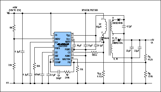
Figure 2. This nonisolated power supply derives 5V/1A from +48V (see design example above).
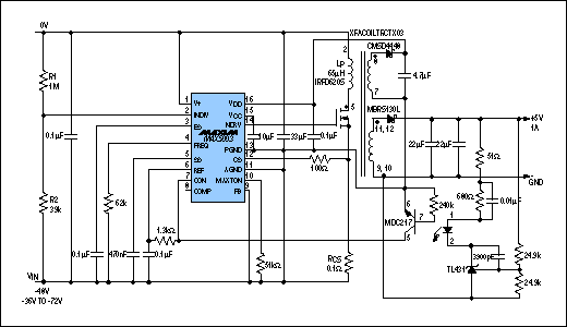
Figure 3. With specifications similar to Figure 2's circuit, this isolated-output supply (-48V to 5V/1A converter) is available from Maxim as a preassembled evaluation kit (MAX5003EVKIT).
 電子發(fā)燒友App






評(píng)論