On Semi公司的RSL10是包含了內置天線,無線電和所需所有無源器件的系統封裝器件(SIP),獲得藍牙特別興趣小組(SIG)認證,無需任何額外的射頻(RF)設計考量,大大減少了上市時間和開發(fā)成本,可實現每秒2兆位 (Mbps)的速度與業(yè)界最低功耗,深度睡眠模式下的功耗僅62.5納瓦(nW),峰值接收功耗僅7毫瓦(mW),主要用IoT邊沿節(jié)點應用兵,可穿戴設備,能量收獲,健身跟蹤/活動監(jiān)測,家用電器,智能手表,心率監(jiān)視器,血糖儀,脈搏血氧計,智能鎖和汽車應用.本文介紹了RSL10主要特性,以及評估板RSL10−002GEVB主要特性,電路圖,材料清單和PCB元件布局圖.
RSL10 is a Bluetooth 5 certified, multi-protocol radio System on Chip (SoC) which brings ultra-low-power Bluetooth Low Energy to wireless applications.
Offering the industry’s lowest power consumption, RSL10 helps provide devices like heart rate monitors with advanced wireless features while optimizing system size and battery life.
Unlike most other multi-protocol radio SoCs, RSL10 is specifically designed for applications using 1.2 and 1.5 V batteries, and supports a voltage supply range between 1.1 and 3.3 V without a required DC/DC converter. The highly-integrated radio SoC features a dual-core architecture and a 2.4 GHz transceiver, providing the flexibility to support Bluetooth Low Energy and 2.4 GHz proprietary or custom protocols.
RSL10主要特性:
Ultra-Low-Power:
- Industry’s lowest power consumption in Deep Sleep Mode (62.5 nW) and Rx in Receive Mode (7 mW)
- Industry’s best EEMBC® ULPMark™ scores (1090 ULPMark CP @ 3 V; 1260 @ 2.1 V)
Advanced Multi-Protocol Wireless Functionality:
- Rx Sensitivity: -94 dBM
- Transmitting Power: -17 to +6 dBm
- Supports Bluetooth Low Energy and 2.4 GHz proprietary/custom protocols
- Supports Firmware Over The Air (FOTA)
Flexible Voltage Supply Range (1.1 and 3.3 V):
Supports devices using 1.2 and 1.5 V batteries without a required external DC/DC converter
Ultra-Miniature:
RSL10 is offered in a 5.50 mm2 WLCSP and a 6 x 6 mm QFN. For added miniaturization, the radio SoC can be integrated into System-in-Package (SiP) solutions which combine RSL10 with a custom ASIC.
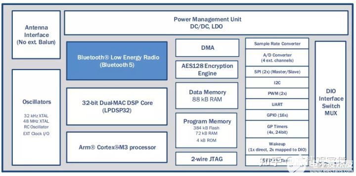
Sophisticated Dual-Core Architecture: Features a programmable ARM Cortex-M3 processor for clocking speeds up to 48 MHz and the flexibility to support 2.4 GHz proprietary and custom protocol stacks. An embedded Digital Signal Processor (DSP) enables signal processing intensive applications, such as wireless audio codecs.
On-Chip and Software Wireless Support: Features a 2.4 GHz Radio Frequency Front-End (RFFE) and a Bluetooth 5 certified baseband controller which supports 2 Mbps data rates. A wide range of supported Bluetooth low energy protocols are provided in the RSL10 development tools kit.
Highly-Integrated System-on-Chip (SoC): The powerful dual-core architecture is complemented by high-efficiency power management units, oscillators, flash, and RAM memories, a DMA controller, and peripherals and interfaces.
Other Key Technical Features:
- 384 kB of flash memory
- IP protection feature to secure flash contents
- Configurable analog and digital sensor interfaces (GPIOs, LSADs, I2C, SPI, PCM)
RSL10應用:
IoT Edge-Node Applications
Bluetooth Low Energy Technology
Wearables
Energy Harvesting
Fitness Trackers/Activity Monitors
Smart Watches
Hearing Aids/Hearables
Heart Rate Monitors
Blood Glucose Monitors (BGM)
Continuous Glucose Monitors (CGM)
Pulse Oximeters
Appliances (e.g., A/C, fans, etc.)
Smart Locks
Lighting Applications
Automotive Applications (Qualification Ready Q4/18)
評估板RSL10−002GEVB
This manual provides detailed information about theconfiguration and use of the RSL10 Evaluation andDevelopment Board (RSL10−002GEVB). The Evaluationand Development Board is designed to be used with thesoftware development tools to evaluate the performance andcapabilities of the RSL10 radio System-on-Chip (SoC).
The RSL10 Evaluation and Development Board is usedfor evaluating the RSL10 SoC and for applicationdevelopment. The board provides access to all input andoutput connections via 0.1″ standard headers. The on-boardcommunication interface circuit provides communication tothe board from a host PC. The communication interfacetranslates RSL10 SWJ−DP debug port signals to the USB ofthe host PC. There is also an on-board 4-bit level shifter fordebugging; it translates the I/O signal level of RSL10 to the 3.3 V digital logic level. It is not enabled by default; youenable it when it is needed.
圖1. 評估板RSL10−002GEVB外形圖
評估板RSL10−002GEVB主要特性:
The Evaluation and Development Board enablesdevelopers to evaluate the performance and capabilities ofthe RSL10 radio SoC in addition to developing,demonstrating and debugging applications.
Key features of the board include:
• J−Link onboard solution provides a SWJ−DP(serial-wire and/or JTAG) interface that enables you todebug the board via a USB connection with the PC
• Alternate onboard SWJ−DP (serial-wire and/or JTAG)interface for ArmR CortexR−M3 processor debugging
• Access to all RSL10 peripherals via standard 0.1″headers
• Onboard 4-bit level translator to translate the LPDSP32debug interface at low voltage to a 3.3 V JTAGdebugger
• Antenna matching and filtering network
• Integrated PCB antenna
• Compliance with the Arduino form factor
• Support for PMOD (i.e., J4 is a standard connector)
![[原創(chuàng)] On Semi RSL10藍牙5多協議無線片上系統(SoC)解決方案](/uploads/allimg/180926/1JF15N0_0.png)
圖2.評估板RSL10−002GEVB電路圖(1)
![[原創(chuàng)] On Semi RSL10藍牙5多協議無線片上系統(SoC)解決方案](/uploads/allimg/180926/1JP1BF_0.png)
圖3.評估板RSL10−002GEVB電路圖(2)
![[原創(chuàng)] On Semi RSL10藍牙5多協議無線片上系統(SoC)解決方案](/uploads/allimg/180926/1JZ111A_0.png)
圖4.評估板RSL10−002GEVB電路圖(3)
![[原創(chuàng)] On Semi RSL10藍牙5多協議無線片上系統(SoC)解決方案](/uploads/allimg/180926/1K0013492_0.png)
圖5.評估板RSL10−002GEVB電路圖(4)
評估板RSL10−002GEVB材料清單:
![[原創(chuàng)] On Semi RSL10藍牙5多協議無線片上系統(SoC)解決方案](/uploads/allimg/180926/1K1011U3_0.png)
![[原創(chuàng)] On Semi RSL10藍牙5多協議無線片上系統(SoC)解決方案](/uploads/allimg/180926/1K2022457_0.png)
![[原創(chuàng)] On Semi RSL10藍牙5多協議無線片上系統(SoC)解決方案](/uploads/allimg/180926/1K4053544_0.png)
圖6.評估板RSL10−002GEVB PCB元件分布圖(頂層)
![[原創(chuàng)] On Semi RSL10藍牙5多協議無線片上系統(SoC)解決方案](/uploads/allimg/180926/1KP244a_0.png)
圖7.評估板RSL10−002GEVB PCB元件分布圖(底層)
![[原創(chuàng)] On Semi RSL10藍牙5多協議無線片上系統(SoC)解決方案](/uploads/allimg/180926/1KZ3V64_0.png)
圖8.評估板RSL10−002GEVB PCB元件3D分布圖(頂層)
![[原創(chuàng)] On Semi RSL10藍牙5多協議無線片上系統(SoC)解決方案](/uploads/allimg/180926/1P00Ec4_0.png)
圖9.評估板RSL10−002GEVB PCB 元件3D分布圖(底層)
詳情請見:
和
RSL10CN-D.PDF
EVBUM2529-D.PDF
 電子發(fā)燒友App






評論