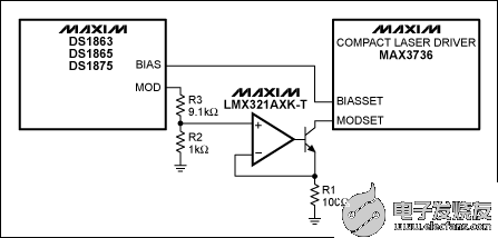
The different modes of electrical interface between a laser driver and the digitally controlled potentiometers and resistors that control it are reviewed in the context of open- and closed-loop operation. The objective in these fiber-optic systems is to vary the amplitude of light using the laser driver's bias and modulation circuits, causing the optical power to swing between two levels (P0 and P1).
Open-Loop Topologies
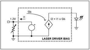
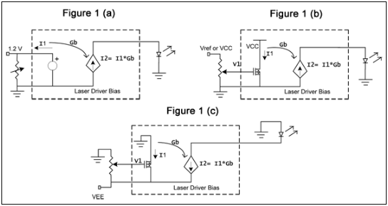
In the bias-control topology of Figure 1a, the variable resistor sets a current (I1) that is amplified and fed to a common-cathode laser diode (or sunk from a common-anode type). The most common voltage across the resistor is 1.2V, which is derived from a bandgap reference internal to the laser driver. I1 ranges from microamperes to a few milliamperes, and I2 ranges from tens of milliamps to 100mA. For some applications in which the resistor sources current, it can be connected to a fixed reference or to the supply instead of ground.Figure 1b shows a low-side circuit (control with respect to ground) in which the input voltage V1 sets an internal current I1, which is amplified to a level of I2 for driving the laser by either sourcing or sinking current. The potentiometer in this circuit is ideal for the high-input impedance seen by V1. (In the Figure 1a configuration, a variable resistor is more appropriate.)
For high-side control (Figure 1c), a decreasing control voltage (V1) causes an increase in I1 and in the laser-drive current I2. Thus, to increase the laser output's average optical power, resistance has to decrease in Figure 1a, V1 has to increase in Figure 1b, and V1 has to decrease in Figure 1c.
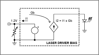 Figure 1a. |
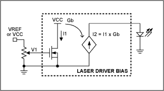 Figure 1b. |
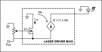 Figure 1c. | |
Figure 1. Open-loop methods for control of laser-bias current include (a) low-side control (laser-cathode grounded) with a variable resistor, or (b) a potentiometer driving a high-impedance input, and (c) high-side control (laser anode grounded) with a negative supply.
Circuit configurations for control of the laser-modulation level (Figures 2a and 2b) are similar to those for control of the bias current. Amplitude modulation of the data carrier produces a switched current. To increase the peak-to-peak amplitude of emitted light, lower the variable resistance in Figure 2a or increase V3 in Figure 2b. (These diagrams show the injection of bias current into the laser as well as modulation current.) In Figure 1b and 2b, note that the input stage of the laser driver IC, which carries I1 or I3, can be a bipolar npn transistor.
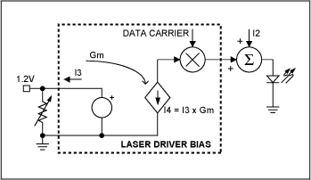 Figure 2a. |
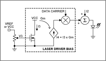 Figure 2b. |
Figure 2. Circuits for low-side control of laser-modulation current are similar to those for control of bias current in Figures 1a and 1b.
Closed-Loop Topologies
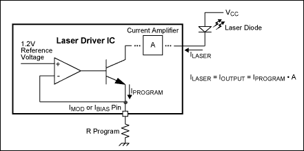
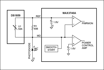
Average power control (APC) is a common means for regulating the average optical output of a laser. The laser is controlled by a photodiode monitor in the feedback path, resulting in closed-loop control of the laser light.Less common are closed-loop modulation-control circuits. Figures 3a and 3b show a resistor interface to such laser drivers.
In Figure 3a, the laser-bias current is an amplified version of the error between the current fed back from the photodiode monitor (Ifa) and a reference current (I1). As the variable resistance decreases, I1 increases. Because If a tracks I1, the average optical power also increases.
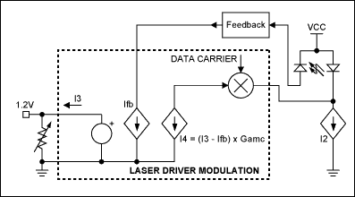
Figure 3b is a simplified representation of closed-loop modulation. Comparing a feedback signal derived from the photodiode current (Ifb) with a reference current (I3) produces an error that is amplified and used to modulate the data-carrier amplitude, resulting in a switched current. As resistance decreases, the peak-to-peak optical power increases. Bias current (I2) is included in Figure 3b to complete the picture.
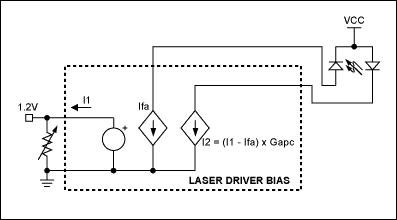 Figure 3a. |
|
Figure 3. (a) A photodiode monitor allowing closed-loop laser control can also accommodate (b) control of the modulation current.
Example:The MAX3273/DS1847 Pair
To interface laser driver MAX3273 to the DS1847 digitally controlled resistor, first determine your average optical power (Pavg) and peak-to-peak optical modulation power (Pmod).Pavg is regulated by an APC loop around the laser driver (Figure 3a), and depends directly on I1 and the photodiode's responsivity in mA/mW. The DS1847 resistor sets I1 equal to 1.2/R. Next, Pavg = I1/responsivity = 1.2/(responsivity × R)
Note the dependence of R on the photodiode characteristic in achieving the required average power. Therefore, to achieve reasonable design yields, it is recommended that the designer know the statistical distribution of this parameter as well as its temperature dependence. For example, A DFB laser (SLT2170-LN) with Pavg = 0.4mW produces a photodiode current that ranges upward from 0.15mA, which in turn calls for <8kΩ; resistance. Resistor 1 internal to the DS1847 should be used for the APC function.
Pmod is not regulated within the laser driver, and therefore runs open loop. It is controlled by a resistor that sets I3 (see Figure 2a). In turn, I3 sets the peak-to-peak modulation current, which is added to the bias current and injected into the laser. As a result, the laser- light output consists of a DC component and a pulsed component. The pulsed component (Pmod) depends on the laser quantum efficiency (η) expressed in mW/mA, the gain Gm (Figure 2a), and I3 (which equals 1.2/Rmod). Thus, Pmod = 1.2 × Gm × h/Rmod.
Again, Rmod depends on η for a given Pmod, so it is important to understand the variation of h. For a system that includes the same laser (SLT2170-LN) with Pmod = 0.6mW, Gm = 165, and η = 0.06, the required resistance is less than 20kΩ;. The DS1847's resistor 0 should be used for the modulation function.
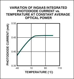
The DS1847 includes look-up tables for temperature compensation (refer to Maxim/Dallas Semiconductor App Note 167: Considerations for the DS1847/1848 Look-Up Tables). Such compensation is essential for the APC and modulation controls. In APC mode the table serves to offset the temperature dependence of photodiode responsivity, which varies as much as ±1.5dB (about 40%) per the SLT2170-LN data sheet. As for modulation, the corresponding table serves primarily to offset temperature dependence of the laser efficiency η, which can vary as much as ±3dB (a factor of 2).
An added benefit of look-up tables is their help in compensating the temperature dependence of laser-driver gain, resistor value, and other parameters in the application. The DS1847 resistor value is characterized at various temperatures in the Dallas factory. The result fits into an equation, whose coefficients are stored in registers for use during calibration at the customer site (refer to Application Note 167).
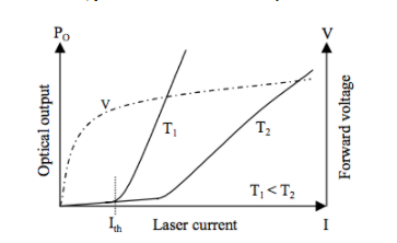
To illustrate some of the concepts described in the previous paragraph, Figures 4a, 4b, and 4c show typical characteristics in lasers and photodiodes after they are temperature compensated with look-up tables.
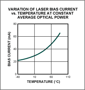
Figure 4a. A laser bias current variation is implemented with a look-up table if an open-loop operation such as Figure 1a is used.
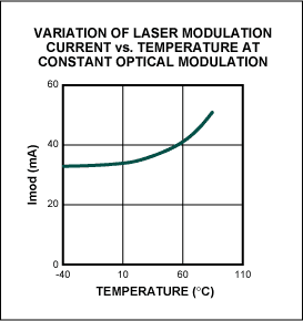
Figure 4b. A peak-to-peak laser modulation current variation is implemented with a look-up table if an open-loop operation, such as Figure 2a, is used.

Figure 4c. An integrated photodiode current variation is implemented with a look-up table if a closed-loop operation (APC), such as Figure 3a, is used.
 電子發(fā)燒友App














評論