Abstract: Application note for interfacing the MAX195 and MAX194 analog-to-digital converters (ADCs) to the TMS320C3X evaluation module. Example demo code is given. The demo software configures the TMS320C30 so that FSR1 and DR1 are inputs and CLKR1 and XF1 are outputs. To read the MAX194/MAX195, the software briefly drives the XF1 output low. The demo software polls the serial receiver until a complete frame has been received. Because this is just an interface demo, the software simply writes the received data word to the EVM host data port.
The example program was assembled using the TMS320C3X/4X COFF Assembler Version 4.50 and the TMS320C3X/4F COFF Linker Version 4.50 (copyright 1987 through 1992 by Texas Instruments Incorporated).
Table 2. Ribbon-Cable Signals
To read the MAX194/MAX195, the software briefly drives the XF1 output low. The demo software polls the serial receiver until a complete frame has been received. Because this is just an interface demo, the software simply writes the received data word to the EVM host data port.
Project: MAX195 EVKIT Interface to TMS320C3X EVM
Project file = MAX195I
Filename = MAX195I.ASM
Command file = MAX195I.CMD
Compile with the following commands:
? ?asm30 MAX195I -l
? ?lnk30 MAX195I.CMD
Pin Assignments:

Note: jumper JU8 must be OPEN
and CS must be tied to GND
Timing Diagram:
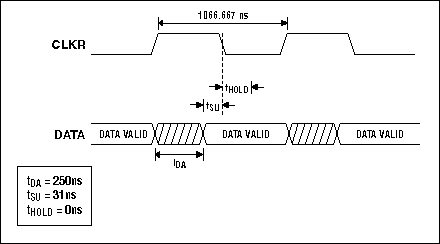
Fastest Clock 1MHz = (1 / 1000 nsec)
Minimum Receiver Timer Period = 4H
Receive Timer Period = 4 = 0.9375MHz
(System clock frequency = 30MHz)
Word diagram:

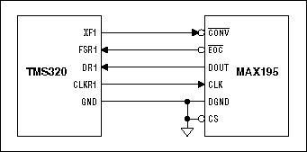
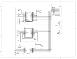
Figure 1. Schematic.
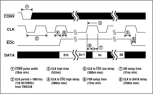
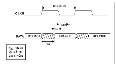
Figure 2. Timing
Overview
The MAX195 16-bit ADC can be interfaced to Texas Instruments' TMS320C30 DSP by means of its serial interface. The interface uses four wires plus ground. This application note explains how to interface the MAX194/MAX195 Evaluation Kit to the TMS320C3X Evaluation Module.The example program was assembled using the TMS320C3X/4X COFF Assembler Version 4.50 and the TMS320C3X/4F COFF Linker Version 4.50 (copyright 1987 through 1992 by Texas Instruments Incorporated).
Interfacing the MAX194/MAX195 EVKIT to the TMS320C3X EVM
Maxim's MAX194/MAX195 Evaluation Kit can be interfaced to Texas Instruments' TMS320C3X Evaluation Module as follows:- Set the MAX194/MAX195 EVKIT jumpers according to Table 1.
- Solder a 2-x-5-pin berg strip into MAX194/MAX195 EVKIT area J3. The PC board is already wired as shown in Table 2.
- Connect a +5V power supply to the MAX194/MAX195 EVKIT.
- Connect a 10-pin ribbon cable between the TMS320C3X EVM and the MAX194/MAX195 EVKIT.
- Run the demo software.
| Jumper | Position | Function |
| JU1 |
|
|
| JU3 |
|
|
| JU4 |
|
|
| JU5 |
|
|
| JU6 |
|
|
| JU7 |
|
|
Table 2. Ribbon-Cable Signals
| Pin | MAX195 | TMS320 | Pin | MAX195 | TMS320 |
| 1 |
|
|
|
|
|
| 3 |
|
|
|
|
|
| 5 |
|
|
|
|
|
| 7 |
|
|
|
|
|
| 9 |
|
|
|
|
|
How It Works
The demo software (see the program-code listing that follows) configures the TMS320C30 so that FSR1 and DR1 are inputs and CLKR1 and XF1 are outputs. The software uses the XF1 output to initiate a conversion. The XF1 pulse drives the MAX194/MAX195 conversion start input. The CLKR1 output provides the conversion clock to the MAX194/MAX195. Data output from the MAX194/MAX195 is received on the DR1 input. The FSR1 Frame Start signal is driven by the MAX194/MAX195 EOC (End of Conversion) signal, which marks the beginning of the serial frame.To read the MAX194/MAX195, the software briefly drives the XF1 output low. The demo software polls the serial receiver until a complete frame has been received. Because this is just an interface demo, the software simply writes the received data word to the EVM host data port.
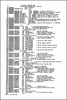
TMS320C3x/4x COFF Assembler, Version 4.50
Copyright (c) 1987-1992, Texas Instruments Incorporated
TMS320C30 Serial Port InitializationProject: MAX195 EVKIT Interface to TMS320C3X EVM
Project file = MAX195I
Filename = MAX195I.ASM
Command file = MAX195I.CMD
Compile with the following commands:
? ?asm30 MAX195I -l
? ?lnk30 MAX195I.CMD
Pin Assignments:

Note: jumper JU8 must be OPEN
and CS must be tied to GND
Timing Diagram:

Fastest Clock 1MHz = (1 / 1000 nsec)
Minimum Receiver Timer Period = 4H
Receive Timer Period = 4 = 0.9375MHz
(System clock frequency = 30MHz)
Word diagram:

 .sect    "vectors"
 reset .word  init
 int0 .word  init
 int1 .word  init
 int2 .word  init
 int3  .word  init
 xint0 .word  init
 rint0  .word  init
 xint1 .word  init
 rint1  .word  init
 tint0 .word  init
 tint1  .word  init
 dint .word  init

   .data
    STCK  .word  0809F00H ; initial stack pointer

    CTRL .word  0808000H ; peripheral interface base address
    HOST_DATA  .word  0804000H ; host data port address

    IOF_AMASK  .set  0000EH ; clear all XF1 bits in IOF register
 IOF_SET_XF1  .set  00060H ; make XF1 pin an output; value = 1
 IOF_RESET_XF1  .set  00020H ; make XF1 pin an output; value = 0
 IOF_INPUT_XF1  .set  00080H ; make XF1 pin an input; read its value

 FS_AMASK  .set  0F0FFH ; mask for an FS pin
 SET_FS  .set  00600H ; make FS a high output
 RESET_FS  .set  00200H ; make FS a low output
 GET_FS  .set  00800H ; input mask for FS pin

 D_AMASK  .set  0FF0FH ; mask for a Data pin
 SET_D  .set  00060H ; make D a high output
 RESET_D  .set  00020H ; make D a low output
 GET_D  .set  00080H ; input mask for D pin

 CLK_AMASK  .set  0FFF0H ; mask for a CLK pin
 SET_CLK  .set  00006H ; make CLK a high output
 RESET_CLK  .set  00002H ; make CLK a low output
 GET_CLK  .set  00008H ; input mask for CLK pin

   Serial Port Global Control Register

 SerGlob1  .word 08100280H

 08000000H:  RRESET - reset / enable the receiver
 0080H:  RCLKSRCE - use internal receive clock (CLKR pin is an output)
 0200H:
  RVAREN - Receiver Variable Data Rate
 00100000H:  RLEN = 2 bytes (16 bits)

   Pin Assignment Register for FSX, CLKX, DX

 SerPrtX1   .word 00H

   assign CLKX pin to general I/O
   make CLKX an input
   assign DX pin to general I/O
   make DX an input
   assign FSX pin to general I/O
   make FSX an input

   Pin Assignment Register for FSR, CLKR, DR

 SerPrtR1   .word 0111H


 0001H:  assign CLKR pin to serial port clock
 0010H:  assign DR pin to serial port receive data
 0100H:  assign FSR pin to serial port frame start

   Serial Port Timer Global Control Register

 SerTim1  .word 03C0H


  XHLD 0=hold transmit timer
  XC/P  0=pulse mode
  XCLKSRC 0=CLKX pin increments the counter
 0040H:  RGO=1 --  start the receive timer
 0080H:  RHLD 1=run receive timer
 0100H:  RC/P  1=clock (50% duty cycle)
 0200H:  RCLKSRC  1=use 7.5MHz time base (30MHz system clock/4)

   Serial Port Timer Period Register

 SerTim1Val   .word 040000H


 0 H:  Transmit Counter Period
 4 H:  Receive Counter Period

   Receive Timer Period = 4 = 0.9375MHz

     .text
 init


 LDI  0,ST  ; initialize status register
 LDI  0,DP  ; point data page pointer into rom
 LDI  @STCK,SP  ; initialize stack pointer

   ; start with XF1 high
   ;


 LDI  IOF,R1  ; get XF1 settings
 AND  IOF_AMASK,R1  ; don't touch XF0 settings
 OR  IOF_SET_XF1,R1  ; make XF1 output a high value
 LDI  R1,IOF  ; write new XF1 settings

   ; initialize serial port
   ;


 LDI  @CTRL,AR0  ; peripheral interface address
 LDI  @HOST_DATA,AR1  ; host interface address

 LDI  @SerTim1Val,R0
 STI  R0,*+AR0(86)  ; serial ch1 timer period

 LDI  @SerGlob1,R0
 STI  R0,*+AR0(80)  ; serial global register

 LDI  @SerPrtX1,R0
 STI  R0,*+AR0(82)  ; serial transmit control register

 LDI  @SerPrtR1,R0
 STI  R0,*+AR0(83)  ; serial receive control register

 LDI  @SerTim1,R0
 STI  R0,*+AR0(84)  ; serial ch1 timer register

 XF1 signal is named Active-Low CONV to MAX195 EVKIT

 This is how we set XF1:


 LDI  IOF,R1  ; get XF1 settings
 AND  IOF_AMASK,R1  ; don't touch XF0 settings
 OR  IOF_SET_XF1,R1  ; make XF1 output a high value
 LDI  R1,IOF  ; write new XF1 settings

 This is how we clear XF1:

 LDI  IOF,R1  ; get XF1 settings
 AND  IOF_AMASK,R1  ; don't touch XF0 settings
 OR  IOF_RESET_XF1,R1  ; make XF1 output a low value
 LDI  R1,IOF  ; write new XF1 settings

 next_sample:

   generate conversion start pulse


 LDI IOF,R1  ; get XF1 settings
 AND IOF_AMASK,R1  ; don't touch XF0 settings
 OR IOF_RESET_XF1,R1  ; make XF1 output a low value
 LDI R1,IOF  ; write new XF1 settings
 AND IOF_AMASK,R1  ; don't touch XF0 settings
 OR  IOF_SET_XF1,R1  ; make XF1 output a high value
 LDI R1,IOF  ; write new XF1 settings

   wait until serial receive is complete

 loop


 LDI *+AR0(80),R2  ; read global control register
 AND 01H,R2  ; test the receiver ready bit
 BZ loop  ; loop until data is received

   get the received data

 LDI *+AR0(92),R3  ; copy received data into R3

 this demo application does no processing --
 it just makes the value available to the
 TMS320C3X EVM's host.

 STI R3,*+AR1(0) ; send R3 to host

 LDI  100,R0  ; delay

 wait_loop:


 SUBI 1,R0
 BNZ  wait_loop

 BR  @next_sample  ; this program runs forever

 .end

Figure 1. Schematic.

Figure 2. Timing
 電子發(fā)燒友App











評論