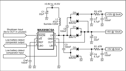
Figure 1. Adding external charge pumps to this 5V boost converter produces auxiliary analog rails of 10V and -5V.
The main regulated output of 5V ±2% is sustained by input voltages in the range 0.8V to 5.5V (i.e., from a battery pack of 1 to 3 cells). With an input of 1.8V (two flat cells) and the other rails unloaded, it can produce 25mA with a high efficiency of 80% to 90%.
The -5V and 10V outputs are derived from low-cost, discrete charge pumps driven by the converter's switching node (LX) via "flying capacitors" C3 and C6. The LX node switches between 0V and a level one diode drop above the 5V rail, so the charge pumps' drive voltage is reasonably well regulated. Moreover, the drop across D1 somewhat compensates for diode drops in the two charge-pump outputs.
Even more useful is the behavior of IC1 with an increasing load on the auxiliary rails. Its internal control scheme (current-limited, minimum-off-time, pulse-frequency modulation) constantly adapts its switching frequency to the net load current drawn from the rails: frequency increases when the load increases, producing a greater transfer of energy via the flying capacitors. The result is a sort of pseudo-regulation for the charge-pump outputs.
These analog supply rails are intended for driving precision op amps, whose input CMR and output range are 2V to 3V within the supply rails. Thus, the rails are good enough if the -5V output is below -3V and the 10V output is above 8V. Accordingly, the components shown were chosen for minimum cost and lowest ripple rather than maximum regulation. Examples are the lossy RC output filters, and the choice of silicon signal diodes instead of Schottky diodes. The 4.7μF capacitors C4 and C7 can be high-ESR, commodity multilayer ceramic types with 16V rating, 1206 case, and Y5V dielectric— such as the 1206YG475ZAT2A from AVX.
Output ripple varies with the supply voltage and output load. Operating with an input voltage of 1.8V, the circuit produces ripple amplitudes over the load range of 2mV to 10mVp-p for the 10V rail and 15mV to 30mVp-p for the -5V rail. By increasing C5 and C8 to 2.2μF, you can reduce these ripple levels to 1mV and 5mV respectively.
With auxiliary rails unloaded, the 5V output's maximum available load current rises with input supply voltage (Figure 2). You can increase this available output power by replacing D1 with a lower-loss Schottky diode. At an input of 1.8V, the output power available for the three rails (loaded with 10mA at 5V, 5mA at 10V, and 5mA at -5V) is 125mW. A 2.7V input based on three flat cells yields 275mW.
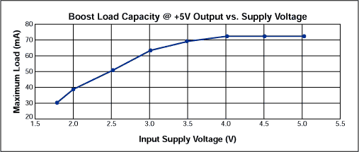
Figure 2. Available load current for the main 5V output in Figure 1 increases with input voltage.
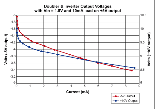
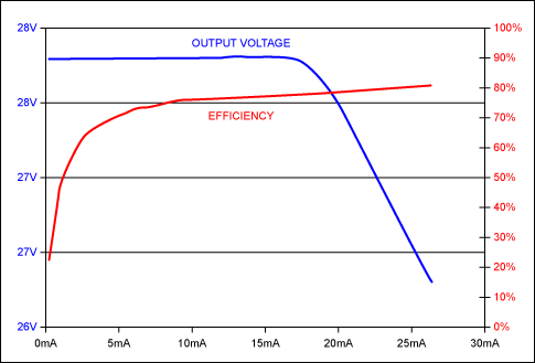
Figure 3. The nominal 10V and -5V aux outputs in Figure 1 vary with output current as shown.
The MAX858 operates with peak inductor currents of 125mA. If you need more current, replace it with a MAX856 (500mA) or a MAX756 (1A), which scale the available output current accordingly. Note that these changes require different passive components: the inductor and main output diode must be rated for the inductor's peak current, but the charge pumps can remain the same if their output currents don't change much.
It's also possible to retain the cheap, common, commodity dual diodes BAV70 and BAV99, but detail specifications vary, so look carefully at data sheets for the parts you actually use. For example, the BAV70's DC forward current (IF) and peak forward surge current (IFSM for 1μs) differ among manufacturers as follows: IF = 200mA; IFSM = 500mA (Motorola), IF = 600mA; IFSM = 2A (National Semiconductor), IF = 125mA; IFSM = 4A (Philips), and IF = 250mA; IFSM = 4.5A (Temic). This caution is probably advisable in all second-source considerations.
Note: Step-up DC-DC converters have improved since this circuit was originally constructed. Consider trying the MAX1724 in this circuit. It's available in a smaller package (SOT23 vs. micromax), consumes significantly less quiescent current, and eliminates diode D1 because it includes a synchronous rectifier. The LX node of this switcher doesn't switch at a diode drop above the output voltage due to the internal synchronous rectifier, however - something that will drop the magnitude of the +10V and -5V outputs by about a diode drop from the voltages achieved using the original DC-DC converter.
 電子發(fā)燒友App








評論