Overview
The DS87C530 and DS5250 incorporate a real-time clock (RTC) and alarm to allow the user to perform real-world timing operations such as time-stamping an event, performing a task at a specific time, or executing very long timing delays. Although software timing loops or internal timers could be used for such measurements, they are crystal dependent, inefficient for long time measurements, and are incompatible with the use of power management modes. Integration of the RTC means that only a 32.768kHz crystal is required. No load capacitors are required with the RTC crystal. The RTC is controlled by dedicated Special Function Registers (SFRs).The RTC consists of subsecond, second, minute, hour, day of the week, and two total day count registers. In addition there is an alarm register for the subsecond, seconds, minutes, and hours registers. The subsecond register provides a resolution of 1/256 of a second and a maximum rollover count of 1 second. The registers and control bits used by the RTC are shown in Table 1. Bits and registers designated as unchanged after a reset may be indeterminate following a no-battery reset. Consult the full bit or register description for complete details.
Table 1. Real-Time Clock Control And Status Bit Summary
| BIT NAME | LOCATION | FUNCTION | RANGE | RESET | READ/WRITE ACCESS |
| ERTCI | EIE.5 | RTC Interrupt Enable | ? | 0 | Unrestricted |
| PRTCI | EIP.5 | RTC Interrupt Priority | ? | 0 | Unrestricted |
| RTASS.7-0 | RTASS | RTC Alarm Subsecond | 0-FFh | Unchanged | Unrestricted |
| RTAS.5-0 | RTAS | RTC Alarm Second | 0-3Bh | Unchanged | Unrestricted |
| RTAM.5-0 | RTAM | RTC Alarm Minute | 0-3Bh | Unchanged | Unrestricted |
| RTAH.4-0 | RTAH | RTC Alarm Hour | 0-17H | Unchanged | Unrestricted |
| RTCSS.7-0 | RTCSS | RTC Subsecond | 0-FFh | Unchanged | Read: only if RTCRE=1. Cannot be written. Cleared when RTCWE 1<0 |
| RTCS.5-0 | RTCS | RTC Second | 0-3Bh | Unchanged | Read: only if RTCRE=1. Write: only if RTCWE=1. 1ms Read/Write window |
| RTCM.5-0 | RTCM | RTC Minute | 0-3Bh | Unchanged | |
| RTCH.4-0 | RTCH.4-0 | RTC Hour | 0-17h | Unchanged | |
| DOW2-0 | RTCH.7-5 | RTC Day of Week | 0-7h | Unchanged | |
| RTCD1.7-0 RTCD0.7-0 |
RTCD1, (MSB) RTCD0, (LSB) |
RTC Day | 0-FFFFh | Unchanged | |
| SRCE | RTCC.7 | RTC Subsecond Compare enable |
? | Unchanged | Unrestricted |
| SCE | RTCC.6 | RTC Second Compare Enable |
? | Unchanged | Unrestricted |
| MCE | RTCC.5 | RTC Minute Compare Enable |
? | Unchanged | Unrestricted |
| HCE | RTCC.4 | RTC Hour Compare Enable |
? | Unchanged | Unrestricted |
| RTCRE | RTCC.3 | RTC Read Enable | ? | 0 | Unrestricted |
| RTCWE | RTCC.2 | RTC Write Enable | ? | 0 | Read: Unrestricted Write: Timed Access |
| RTCIF | RTCC.1 | RTC Interrupt Flag | ? | 0 | Unrestricted |
| RTCE | RTCC.0 | RTC Enable | ? | Unchanged | Read: Unrestricted Write: Timed Access |
| E4K | TRIM.7 | External 4096Hz RTC Signal Enable |
? | 0 | |
| X12/ /6\ | TRIM.6 | RTC Crystal Capacitance Select |
? | Unchanged | |
| TRM2-0 | TRIM.5 TRIM.3 TRIM.1 |
RTC Trim Bit 2-0 | ? | Unchanged | Read: Unrestricted Write: Timed Access |
| /0 - TRM2\ | TRIM.4 TRIM.2 TRIM.0 |
RTC Inverted Trim Bit 2-0 |
? | Unchanged | Read: Unrestricted Write: Timed Access Must be inverse of TRM2-0 |
Both user software and the internal clock directly write and read the RTC time registers (RTCSS, RTCS, RTCM, RTCH, RTCD0, RTCD1). To prevent the possibility of both user software and the internal timer accessing the same register simultaneously, the DS87C530 incorporates a register locking mechanism. Updates to the RTC time registers by the internal timer are temporarily suspended for up to 1ms during software read or write operations. If a subsecond timer tick should occur in the 1ms window, it will be processed immediately as soon as either the RTCWE or RTCRE bits are cleared. To prevent the possibility of an accidental write to the RTC time registers, the RTCWE bit should be cleared as soon as the planned modifications are complete. As a protective measure, the device will clear the RTCWE bit automatically after 1ms if it has not been cleared in software. To allow any pending timer ticks to be processed, software must wait four machine cycles between any successive modifications of the RTCWE or RTCRE bits.
This scheme will not affect the accuracy of the RTC, as any subsecond timer tick that may occur during the read or write window is only temporarily delayed, not discarded. Only the recognition of that single subsecond timer tick is delayed, and subsequent ticks will be synchronized with the clock. The only possible implication with respect to RTC operation occurs if a timer tick that would cause an alarm interrupt occurred during a time register read operation. In that case, the alarm would be delayed a fraction of a millisecond until the RTCRE bit was cleared. As mentioned, the next subsecond timer tick will occur at the proper time, so the long-term clock accuracy will not be affected.
It is critical that the 4-machine cycle setup and 1ms window timings be observed. Any reads from the time registers before the 4-machine cycle period may return an invalid time. Writes to the time registers before the 4-machine cycle period will be ignored. Similarly, any RTC time register operations outside of the 1ms window will result in invalid read operations or ignored write operations. For this reason, interrupts should be globally disabled before modifying any RTC register.
Starting And Stopping The RTC
The operation of the RTC crystal amplifier is controlled by the RTC Enable bit, RTCE (RTCC.0). This bit can only be accessed by a Timed Access procedure and is unaffected by any operational reset. The state of the RTCE bit is undefined after a no-battery reset, however, and should be initialized. Clearing the RTC Enable bit will halt operation of the crystal amplifier and the clock, but all register values (including the time when the clock was disabled) will be retained. This may be desirable to preserve the life of the backup energy source during periods of storage. When restarting the RTC crystal oscillator, either from a no-battery reset condition or by setting the RTC Enable bit, the crystal start-up time must be observed. There is no direct way to detect when the RTC crystal oscillator has stabilized, and the system software must allow sufficient stabilization time when restarting the RTC. Crystal startup times are specified by the crystal manufacturer, but are usually on the order of 1 second.After a loss of battery power or when attaching a battery for the first time it will be necessary to initialize the RTC. Although there is no status bit to indicate a no-battery reset, there are several ways to detect when the real-time clock has lost power/time. The best way is to monitor a reserved location in on-board memory. Because the on-chip SRAM contents are preserved by the same energy source as the RTC, an unexpected change in a previously loaded memory location can indicate a loss of battery power.
Reading The Time
Reading the current time from the RTC is accomplished by the following procedure:- Disable all interrupts by clearing the EA bit (IE.7)
- Set the RTCRE bit (RTCC.3)
- Wait 4 machine cycles
- Read the appropriate register(s) within 1ms of RTCRE being set
- Clear the RTCRE bit (RTCC.3)
- Enable interrupts by setting the EA bit (IE.7)
Setting The Time
The time is set by writing to the Clock Registers. The Second, Minute, Hour, Day of the Week, and Day Count can be set by writing to the respective registers. It is not possible to set the Real-time Clock Subsecond Register (RTCS; FBh). This register is automatically reset to 00h when the RTCWE bit is cleared, either through software or the automatic time-out of the 1ms write window. The procedure for setting an RTC time register is as follows:- Disable all interrupts by clearing the EA bit (IE.7)
- Perform a Timed Access procedure
- Set the RTCWE bit (RTCC.2)
- Wait 4 machine cycles
- Write the appropriate register(s) within 1ms of RTCWE being set
- Perform a Timed Access procedure
- Clear the RTCWE bit (RTCC.2)
- Enable interrupts by setting the EA bit (IE.7)
Using The RTC Alarm
The RTC alarm function is used to generate an interrupt when the RTC value matches selected alarm register values. An alarm can be triggered by a match on one or more of the following alarm registers: Subsecond (RTASS;F2h), Second (RTAS; F3h), Minute (RTAM; F4h), and Hour (RTAM; F5h). Note that there is no alarm register associated with the RTC Day or Day of Week Registers. If an alarm is desired on a specific date, an alarm can be executed once a day and user software can compare the current date against the Day Register. It is not necessary to set the RTC Write Enable bit when setting the alarm registers.The alarm can be set to occur on a match with any or all of the alarm registers. An alarm can occur on a unique time of day, or a recurring alarm can be programmed every subsecond, second, minute, or hour. The specific alarm registers to be compared are selected by setting or clearing the corresponding compare enable bits (RTCC.7-4). Any compare bit which is cleared will result in that register being treated as a 'Don't Care' when evaluating alarm conditions. Clearing all the compare enable bits will disable the ability of the RTC to cause an interrupt, and will immediately clear the RTC Interrupt Flag (RTCC.1). Unlike some interrupts, the RTC flag is not cleared by exiting the RTC interrupt service routine and must be done in software.
The general procedure for setting the RTC alarm registers to cause a RTC interrupt is as follows:
- Clear the RTC Interrupt Enable bit (EIE.5)
- Clear all RTC Alarm Compare enable bits (ANL RTCC, #0Fh)
- Write one or more RTC Alarm registers
- Set the desired RTC Alarm Compare enable bits
- Set the RTC Interrupt Enable bit (EIE.5)
- Setting the alarm to cause an interrupt for a single time during a 24-hour period is done by setting all the alarm registers to the desired value and enabling all compare bits. For example, if an alarm was desired at 11:45:00 am, the following configuration would be used:
Alarm Subsecond (RTASS) 00 subseconds = 00h Alarm Second (RTAS) 00 seconds = 00h Alarm Minute (RTAM) 45 minutes =2Dh Alarm Hour (RTAH) 11 hours =0Bh Clock Control (RTCC) subsecond compare = F1h ? second compare ? ? minute compare ? ? hour compare ?
In the above example, the subsecond, second, and minute registers are programmed and the corresponding compare enable bits are set, even though only a match on the minute register is desired. This is because a don't care is always treated as a match for the purposes of evaluating alarms. If the SSCE and SCE bits were cleared to 0 (don't care) in the above example, then a match (and interrupt) would occur during every subsecond of the minute in which the RTAM register matched. This would cause 15,360 interrupts, which is most likely not the desired effect. In general, when specifying a recurring alarm, all the compare bits below the largest time increment should be enabled and the corresponding alarm registers loaded with 00h or a known value.
Alarm Subsecond (RTASS) 00 subseconds = 00h Alarm Second (RTAS) 00 seconds = 00h Alarm Minute (RTAM) 30 minutes = 1Eh Alarm Hour (RTAH) 11 hours =00h Clock Control (RTCC) subsecond compare = E1h ? second compare ? ? minute compare ? ? RTC enable ?
Alarms can occur synchronously when the clock rolls over to match the alarm condition or asynchronously if the alarm registers are set to a value that matches the current time. Note that only one alarm may occur per subsecond tick. This means that if a synchronous alarm has already occurred during the current subsecond, software cannot cause an asynchronous alarm in the same subsecond.
While this is a relatively minor point, it can have implications if software expects to use the asynchronous capabilities of the alarm. For example, assume an RTC interrupt occurs as when the alarm registers match the current time a 01:00:00:00 (1 hour, 0 minutes, 0 seconds, 0 subseconds). The RTC interrupt is relatively short, taking much less than one subsecond tick (< 4ms), and execution returns to the main program. Immediately upon exiting the RTC interrupt routine, an event occurs that requires software to cause an alarm on the hour by setting the alarm to match on 00 minutes, 00 seconds, 00 subseconds. Normally, setting this alarm condition with the time at 01:00:00:00 would immediately cause an RTC interrupt to occur; but because we have already had an alarm in this subsecond, the condition will not be recognized. The alarm will be missed because it will not be evaluated until the next subsecond tick, when the time will have changed to 01:00:00:01. The designer should guard against the possibility of using synchronous asynchronous alarms in the same subsecond.
Because an alarm condition can occur asynchronously, care must be exercised that a match is not accidentally enabled while writing to the alarm registers. For example, assume that the current time is 0B:00:00:00 and the current alarm conditions are 00:00:00:00. Suppose that software changes the alarm to 0B:01:00:00. If the hour, second, minute, and subsecond compare enables are enabled and the first instruction is MOV RTCH, #0B0H, an alarm will occur immediately instead of at the intended time. The best way to avoid this is to disable all compare enables before changing the RTC alarm registers.
RTC Software Tricks
There are a number of simple tricks that can be used to simplify software associated with RTC operations. The 4-machine cycle delay can be performed using a CJNE A,A,$ instruction. Compared to using 4 NOPs, this is a single instruction, and is 1 byte shorter.The RTC allows software to dynamically vary the alarm registers to achieve a wide range of intervals. Often software will want to interrupt regularly on half-increments of time (every 30 seconds, 30 minutes, etc.). This can be easily done using the XRL instruction. For example, if the RTAM register is set to 00h, the instruction XRL RTAM, #1Eh will change the contents to 1Eh. Performing the instruction again will change it back to 00h. Placing this instruction at the start of the RTC interrupt routine will cause the appropriate alarm register to be easily and quickly modified each time the interrupt is called.
Program Example: DATALOGGER
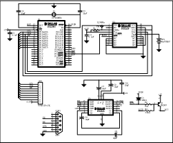
The following program illustrates a generic scheme for operating a remote data logging station. In this example, a DS87C530 is awakened from Stop mode every 30 minutes to read the temperature from a Dallas Semiconductor DS1620 Digital Thermometer and Thermostat. The DS1620 is addressed via serial port 0, using serial mode 0. When the interrupt is called, the DS87C530 will use the ring oscillator to perform a fast resume from Stop and signal the thermostat to begin a temperature conversion. It will then reset the RTC alarm to occur again in 1 second. This will allow time for the conversion and the crystal warm-up period to complete, after which the device will automatically switch back to the crystal as the clock source. The DS87C530 will read the temperature and transmit it, along with the hour and minute, back to a host system connected to serial port 1. It will then return to Stop mode to await the next alarm. Figure 1 shows a partial schematic for interfacing the DS87C530 and DS1620. If the DS1620 is to be separated from the microcontroller by a long distance, filtering may be necessary on the clock and data lines to reduce noise.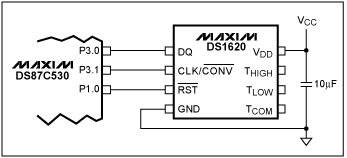
Figure 1. DS1620 interface example.
;Program DATALOGR.ASM
;
;This program demonstrates how to use the RTC to periodically service an
;external device. The device halts in Stop mode until awoken by an RTC interrupt
;every half hour. It then reads the temperature from a DS1620 Digital
;Thermostat and transmits it, with a time stamp, to the host via serial port 1.

;Register equate table
SP equ 81h ;Stack Pointer
PCON equ 87h ;Power Control Register
TCON equ 88h ;Timer Control Register
TMOD equ 89h ;Timer Mode Register
TH1 equ 8Dh ;Timer 1 MSB
CKCON equ 8Eh ;Clock Control Register
P1 equ 90h ;Port 1
EXIF equ 91h ;External Interrupt Flag Register
SCON0 equ 98h ;Serial Port 0 Control Register
SBUF0 equ 99h ;Serial Port 0 Data Buffer
P3 equ 0B0h ;Port 3
SCON1 equ 0C0h ;Serial Port 1 Control Register
SBUF1 equ 0C1h ;Serial Port 1 Data Buffer
TA equ 0C7h ;Timed Access Register
WDCON equ 0D8h ;Watchdog Control Register
ACC equ 0E0h ;Accumulator
RTASS equ 0F2h ;Real-time Alarm Subsecond Register
RTAS equ 0F3h ;Real-time Alarm Second Register
RTAM equ 0F4h ;Real-time Alarm Minute Register
RTCC equ 0F9h ;Real-time Clock Control
RTCM equ 0FCh ;Real-time Clock Minute Register
RTCH equ 0FDh ;Real-time Clock Hour Register

;Bit equate table
RI0 equ 098h
TI0 equ 099h
REN0 equ 09Ch
EA equ 0AFh
TI1 equ 0C1h
ERTCI equ 0Edh

DS1620_RST equ 090h ;DS1620 reset pin is tied to DS87C530 P1.0.
WR_CONFIG equ 0Ch ;DS1620 Write Configuration command.
RD_TEMP equ 0AAh ;DS1620 Read Temperature command.
START_CONV equ 0EEh ;DS1620 Start Conversion command.

cseg at 0 ;Reset vector.
LJMP START
cseg at 6Bh ;Real-time clock Interrupt vector.
LJMP RTC_INT
;
cseg at 100H ;Beginning of code segment.

START: MOV SP, #40h ;Initialize Stack pointer.
MOV EXIF, #0Ah ;Enable ring oscillator restart from Stop mode.
MOV P3, #03h ;Set P3.1 & P3.0 high to use serial port 0.
MOV SCON0, #20h ;Set serial port mode 0, 4 tclk.

MOV P1, #0Ch ;Set P1.2 & P1.3 high to use serial port 1.
;Clear P1.0 to reset DS1620.
MOV SCON1, #40h ;Set serial port mode 1.
MOV TMOD, #20h ;Configure timer 1 for 9600 baud
MOV TH1, #0FDh ; at 11.0592MHz.
MOV TCON, #40h ;Start timer.
;Configure the DS1620
SETB DS1620_RST ;Remove DS1620 reset to start operation.
MOV A, #WR_CONFIG ;Send command to address configuration byte.
CALL OUT_1620
MOV A, #03h ;Set Configuration byte = CPU & 1-Shot Mode.
CALL OUT_1620
CLR DS1620_RST ;Assert DS1620 to end operation.

;Set up the RTC
MOV RTAM, #00h ;Clear all alarm registers. Alarm will ring
MOV RTAS, #00h ; on the next hour to start temperature
MOV RTASS, #00h ; conversion.
MOV RTCC, #081h ;Set alarms so we get a reading at start.
SETB ERTCI ;Enable RTC interrupt.
SETB EA ;Global interrupt enable.

MAIN: ORL PCON, #02h ;Set STOP bit to enter Stop mode.
JMP MAIN ;End of main program loop. Program will return
; here after RTC interrupt is complete.

;***************************************************************************
;RTC_INT - This ISR reads the temp from the DS1620 and outputs the data to
; serial port 1. The routine starts the conversion, and waits for 1
; second to allow conversion to complete and crystal to stabilize.
; When the conversion is complete, the device will read the temperature
; and send the hour, minute and temperature to the host. The RTAM
; register will be modified to alarm again in 30 minutes.
;***************************************************************************
RTC_INT: MOV RTCC, #081h ;Clear RTCI flag and second compare enable
; bit to generate another alarm in 1 second.
PUSH ACC ;Save accumulator.

SETB DS1620_RST ;Remove DS1620 reset to start operation.
MOV A, #START_CONV ;Initiate first temp conversion.
CALL OUT_1620
CLR DS1620_RST ;Assert DS1620 to end operation.
ORL RTCC, #08h ;Enable RTC read process, and delay 4 machine
CJNE A, ACC, $ ; cycles for time registers to stabilize.
MOV R7, RTCM ;Save minute and hour so we can transmit
MOV R6, RTCH ; them as soon as crystal has stabilized.
ANL RTCC, #0F7h ;Reenable time register updates.

WAIT: MOV A, RTCC ;Wait for RTC interrupt flag to be set,
JNB ACC.1, WAIT ; indicating that conversion is done. The
; one second delay will be sufficient for the
; crystal to stabilize, so switch to it now.
XRL RTAM, #1Eh ;Change alarm to ring on next half hour.
MOV RTCC, #0E1h ;Clear RTCI flag, and set compare bits
; so next alarm will be generated in 30 min.
MOV A, #'!' ;Transmit start character.
CALL OUT_HOST

MOV A, R6 ;Transmit the hour.
CALL OUT_HOST
MOV A, R7 ;Transmit the minute.
CALL OUT_HOST

SETB DS1620_RST ;Remove DS1620 reset to start operation.
MOV A, #RD_TEMP ;Conversion is done. Send command to read temp.
CALL OUT_1620
CALL IN_1620 ;Read LSB of temperature and send it to host.
CALL IN_1620 ;Read MSB of temperature and send it to host.
CLR DS1620_RST ;Assert DS1620 to end operation.

POP ACC ;Restore accumulator and go back to sleep.
RETI

;************************************************************************
;OUT_HOST - This routine sends data to the host system via serial port 1.
;************************************************************************
OUT_HOST: MOV SBUF1, A ;Move out byte.
JNB TI1, $ ;Wait until data has been transmitted.
CLR TI1 ;Clear TI1.
RET

;************************************************************************
;OUT_1620 - This routine sends data to the DS1620 via serial port 0.
;************************************************************************
OUT_1620: MOV SBUF0, A ;Move out byte.
JNB TI0, $ ;Wait until data has been transmitted.
CLR TI0 ;Clear TI1.
RET

;************************************************************************
;IN_1620 - This routine reads a byte from the DS1620 and echoes it back
; through serial port 1.
;************************************************************************
IN_1620: SETB REN0 ;Enable receiver to clock in data.
JNB RI0, $ ;Wait until data has been received.
CLR REN0 ;Disable receiver to prevent reception.
CLR RI0 ;Clear RI.
MOV A, SBUF0 ;Echo data through serial port 1.
CALL OUT_HOST
RET
Program Example: RTC Interface
The following program is a general purpose interface routine to set the RTC and display its status. The program communicates through serial port 0, and allows the user to set the time and date, set the alarm registers, and indicates when an alarm has occurred. For the sake of simplicity, the program inputs decimal values of time and outputs hexadecimal values.;*************************************************************************** ;Program RTC_UTIL.ASM ; ;This program responds to commands received over the serial port to set ;and read the date, time and alarm information in the DS87C530 Real-time Clock. ;The program initializes the serial port for operation at 28800 baud with an ;11.0592MHz clock. ;*************************************************************************** ;Register equate table SP equ 81h ;Stack Pointer DPL equ 82h ;Data pointer low register DPH equ 83h ;Data pointer high register PCON equ 87h ;Power Control Register TCON equ 88h ;Timer Control Register TMOD equ 89h ;Timer Mode Register TH1 equ 8Dh ;Timer 1 MSB EXIF equ 91h ;External Interrupt Flag Register SCON0 equ 98h ;Serial Port 0 Control Register SBUF0 equ 99h ;Serial Port 0 Data Buffer P3 equ 0B0h ;Port 3 TA equ 0C7h ;Timed Access Register ACC equ 0E0h ;Accumulator B equ 0F0h ;B Register RTASS equ 0F2h ;Real-time Alarm Subsecond Register RTAS equ 0F3h ;Real-time Alarm Second Register RTAM equ 0F4h ;Real-time Alarm Minute Register RTAH equ 0F5h ;Real-time Alarm Hour Register EIP equ 0F8h ;Extended Interrupt Priority Register RTCC equ 0F9h ;Real-time Clock Control RTCSS equ 0FAh ;Real-time Clock Subsecond register RTCS equ 0FBh ;Real-time Clock Second RTCM equ 0FCh ;Real-time Clock Minute RTCH equ 0FDh ;Real-time Clock Hour RTCD0 equ 0FEh ;Real-time Clock Day Register 0 RTCD1 equ 0FFh ;Real-time Clock Day Register 1 ;Bit equate table RI0 equ 98h ;Serial Port 0 Receiver Interrupt Flag TI0 equ 99h ;Serial Port 0 Transmitter Interrupt Flag EA EQU 0AFh ;Global Interrupt Enable. ERTCI equ 0EDh ;Real-time Clock Interrupt Enable. ;Constant equate table CR equ 0Dh LF equ 0Ah cseg at 0 ;Reset vector. LJMP START cseg at 6BH ;Real-time clock Interrupt vector. LJMP RTC_INT cseg at 100H ;Beginning of code segment. ;Data & string tables. HEX_TABLE: DB '0123456789ABCDEF' NEW_LINE: DB CR, LF, 0 YES: DB 'Y ', 0 N DB 'N ', 0 COMPARE: DB CR, LF, 'Compare enabled: ', 0 COMPARE_Q: DB ' Enable compare (Y/N)? ', 0 ALARM_MSG: DB CR, LF, 'Alarm: ', 0 TT_BANNER: DB CR, LF, CR, LF, 'DS87C530 RTC UTILITY' DB CR, LF, ' A - Set Alarm, T -Set Time' DB CR, LF, ' any other key to show registers' DB CR, LF, CR, LF, 'RTC registers: ', 0 ALM_BANNER: DB CR, LF, 'Alarm register: ', 0 NEW_BANNER: DB CR, LF, CR, LF, 'Enter new alarm register settings:',0 SET_BANNER: DB CR, LF, 'Enter new time:', 0 SS_BANNER: DB CR, LF, 'Subsecond: ', 0 S_BANNER: DB CR, LF, 'Second: ', 0 M_BANNER: DB CR, LF, 'Minute: ', 0 H_BANNER: DB CR, LF, 'Hour: ', 0 DW_BANNER: DB CR, LF, 'Day of Week: ', 0 DC_BANNER: DB CR, LF, 'Day Count: ', 0 DW_STRING: DB 'Disabled ',0,'Sunday ',0,'Monday ',0,'Tuesday ', 0 DB 'Wednesday',0,'Thursday ',0,'Friday ',0,'Saturday ', 0 ;Initialize part. START: MOV SP, #80h ;Set up stack pointer. MOV P3, #0Bh ;Set RXD0, TXD0 & INT1 as inputs. MOV RTAM, #00h ;Initialize alarm registers to known values. MOV RTAS, #00h MOV RTASS, #00h MOV TA, #0AAh ;Timed access write to enable RTC. MOV TA, #55h MOV RTCC, #01h MOV SCON0, #050h ;Set serial port 0 for Mode 1, divide by 12. MOV TH1, #0FEh ;Timer 1 value for 28800 baud at 11.0592MHz. MOV TMOD, #20h ;Set timer 1 to 8-bit auto reload and start it. MOV TCON, #40h ORL PCON, #80h ;Set SMOD bit to get 28800 baud. SETB ERTCI ;Enable RTC interrupts. SETB EA LJMP TELL_TIME ;Display the time. ;*************************************************************************** ;This is the main program loop. It waits for a character on serial port 0, ;and then takes the appropriate action. ;*************************************************************************** CHAR_TEST: JNB RI0, $ ;Wait for incoming command character. CLR RI0 MOV A, SBUF0 ;Test to see what to do. CHECKT: CJNE A, #'T', CHECKA ;T - set time. LJMP SET_TIME CHECKA: CJNE A, #'A', TT_JUMP ;A - set alarm. LJMP SET_ALARM TT_JUMP: LJMP TELL_TIME ;else display time. ;*************************************************************************** ;SET_TIME sets the current time. ;*************************************************************************** SET_TIME: MOV DPTR, #SET_BANNER ;Display set time banner. CALL OUT_STRING MOV DPTR, #H_BANNER ;Get hour & save temp copy. CALL OUT_STRING CALL IN_TIME ANL A, #1Fh ;Make sure day of week bits are 0. MOV R4, A MOV DPTR, #M_BANNER ;Get minute & save temp copy. CALL OUT_STRING CALL IN_TIME MOV R5, A MOV DPTR, #S_BANNER ;Get second & save temp copy. CALL OUT_STRING CALL IN_TIME MOV R6, A MOV DPTR, #DC_BANNER ;Get day count(2 bytes) & save temp copies. CALL OUT_STRING CALL IN_TIME MOV R2, A CALL IN_TIME MOV R3, A MOV DPTR, #DW_BANNER ;Get day of week value and add it on to CALL OUT_STRING ; the upper 3 bits of the hour register. CALL IN_TIME SWAP A RL A ANL A, #0E0h ORL A, R4 XCH A, R4 MOV DPTR, #NEW_LINE ;Add a blank line for esthetics. CALL OUT_STRING MOV TA, #0AAh ;We have all the values, now save them. MOV TA, #055h ;Perform a timed access to write to ORL RTCC, #04h ; set new time & date. CJNE A, ACC, $ ;Delay 4 machine cycles. MOV RTCSS, R7 MOV RTCS, R6 MOV RTCM, R5 MOV RTCH, R4 MOV RTCD0, R3 MOV RTCD1, R2 MOV TA, #0AAh ;Clear RTCWE bit to prevent accidental MOV TA, #055h ; changes to time registers. ANL RTCC, #0FBh LJMP CHAR_TEST ;Return and wait for another event. ;*************************************************************************** ;TELL_TIME displays the current time, alarm registers, and alarm status. ;*************************************************************************** TELL_TIME: MOV DPTR, #TT_BANNER ;Display current time. CALL OUT_STRING CALL OUT_TIME MOV DPTR, #ALM_BANNER;Display alarm registers. CALL OUT_STRING MOV R7, RTASS MOV R6, RTAS MOV R5, RTAM MOV R4, RTAH CALL DISP_TIME MOV DPTR, #COMPARE ;Now display the compare bits. CALL OUT_STRING MOV A, RTCC CALL DISP_COMP ;Display Hour compare bit. RR A CALL DISP_COMP ;Display Minute compare bit. RR A CALL DISP_COMP ;Display Second compare bit. RR A CALL DISP_COMP ;Display Subsecond compare bit. ORL RTCC, #08h ;Set the read bit to stop RTC update. CJNE A, ACC, $ ;Delay 4 machine cycles. MOV R4, RTCH ;Read the hour register. MOV R3, RTCD0 ;Read the day count registers. MOV R2, RTCD1 ANL RTCC, #0F7h ;Clear the read bit to restart RTC. MOV DPTR, #DW_BANNER ;Output Day of Week banner. CALL OUT_STRING ; the upper 3 bits of the hour register. MOV A, R4 ;Day of week is stored in upper 3 bits SWAP A ; of hour register. Move it to bits 2-0 RR A ; and multiply by 10 to get location ANL A, #07h ; within day of week table to start. MOV B, #0Ah MUL AB MOV DPTR, #DW_STRING ;Now add offset to starting address ADD A, DPL ; of data table to calculate new JNC NO_INC ; data pointer location. INC DPH NO_INC: MOV DPL, A CALL OUT_STRING MOV DPTR, #DC_BANNER ;Output day count banner. CALL OUT_STRING MOV A, R2 ;Send both registers of day count. CALL OUT_DIGIT MOV A, R3 CALL OUT_DIGIT MOV DPTR, #NEW_LINE ;Add a blank line for aesthetics. CALL OUT_STRING LJMP CHAR_TEST ;Return and wait for another event. ;This routine displays the status of the compare enable bit. DISP_COMP: JNB ACC.4, NO_COMP ;Display the hour compare bit. MOV DPTR, #YES JMP OUT_COMP NO_COMP: MOV DPTR, #NO OUT_COMP: CALL OUT_STRING RET ;This routine outputs the current time. OUT_TIME: ORL RTCC, #08h ;Set the read bit to stop RTC update. CJNE A, ACC, $ ;Delay 4 machine cycles. MOV R7, RTCSS ;Grab the current time / date and store MOV R6, RTCS ; them temporarily in working registers. MOV R5, RTCM MOV R4, RTCH ANL RTCC, #0F7h ;Clear the read bit to restart RTC. DISP_TIME: MOV A, R4 ;Output hour. ANL A, #01Fh ;Mask off day of week bits. CALL OUT_DIGIT MOV A, R5 ;Output Minute. CALL OUT_CDIGIT MOV A, R6 ;Output second. CALL OUT_CDIGIT MOV A, R7 ;Output subsecond. CALL OUT_CDIGIT RET ;*************************************************************************** ;SET_ALARM sets the alarm registers. ;*************************************************************************** SET_ALARM: CLR ERTCI ;Disable RTC interrupt and clear flag ANL RTCC, #0Fh ; during this section so that alarms will ; not be called while enables are changing. MOV DPTR, #NEW_BANNER CALL OUT_STRING MOV DPTR, #H_BANNER CALL OUT_STRING CALL IN_TIME ;Get hour & save temp copy. MOV R4, A CALL QUERY JNC ASK_M ORL RTCC, #10h ;Enable hour compare ASK_M: MOV DPTR, #M_BANNER CALL OUT_STRING CALL IN_TIME ;Get minute & save temp copy. MOV R5, A CALL QUERY JNC ASK_S ORL RTCC, #20h ;Enable minute compare ASK_S: MOV DPTR, #S_BANNER CALL OUT_STRING CALL IN_TIME ;Get second & save temp copy. MOV R6, A CALL QUERY JNC ASK_SS ORL RTCC, #40h ;Enable second compare ASK_SS: MOV DPTR, #SS_BANNER CALL OUT_STRING CALL IN_TIME ;Get subsecond & save temp copy. MOV R7, A CALL QUERY JNC ASK_X ORL RTCC, #80h ;Enable subsecond compare. ASK_X: MOV DPTR, #NEW_LINE CALL OUT_STRING MOV RTASS, R7 ;Save new alarm values. MOV RTAS, R6 MOV RTAM, R5 MOV RTAH, R4 ANL RTCC, #0FDh ;Clear the RTCI flag in case it was ; accidentally set while we were ; manipulating compare bits. SETB ERTCI ;Reenable RTC interrupt. LJMP CHAR_TEST QUERY: MOV DPTR, #COMPARE_Q CALL OUT_STRING JNB RI0, $ CLR RI0 MOV A, SBUF0 CALL OUT_CHAR ;Echo it. CJNE A, #'Y', NO_ENABLE ;If user wants compare, set flag. SETB C RET NO_ENABLE: CLR C ;User does not want compare, clear flag. RET ;****************************************************************** ;Output routines. ;****************************************************************** ;This subroutine outputs an ASCII string. The starting point of the string ;is in DPTR, and the terminating character is '0'. OUT_STRING: PUSH ACC ;Save accumulator. CHAR_LOOP: CLR A ;Clear accumulator for next instruction. MOVC A, @A + DPTR Get the next character from the JNZ NXT_CHAR ; string, and if 0, exit. POP ACC ;Restore accumulator. RET NXT_CHAR: CALL OUT_CHAR ;Next character is valid, so transmit INC DPTR ; it. Increment the data pointer JMP CHAR_LOOP ; to the next position and loop ; back to send character. ;This subroutine outputs a leading colon for the minute, second, and subsecond ; when displaying the time. When done, it falls through to OUT_DIGIT. OUT_CDIGIT: MOV SBUF0, #':' ;Display a colon. JNB TI0, $ CLR TI0 ;This subroutine outputs a hex number in ASCII format through serial port 0. OUT_DIGIT: MOV DPTR, #HEX_TABLE MOV R0, A ;Make another copy of value SWAP A ;Do high nibble fist ANL A, #0Fh ;Clear unused nibble MOVC A, @A+DPTR ;Get character from table CALL OUT_CHAR ;Transmit the character. MOV A, R0 ;Now do low nibble. ANL A, #0Fh ;Clear unused nibble MOVC A, @A+DPTR ;Get character from table CALL OUT_CHAR ;Transmit the character. RET ;Done OUT_CHAR: MOV SBUF0, A ;Transmit the character out the serial JNB TI0, $ ; port and wait until complete. CLR TI0 RET ;****************************************************************** ;Input routines. ;****************************************************************** ;IN_TIME takes two decimal characters from the serial port, and formats them ; as a hexadecimal number. IN_TIME: CALL IN_CHAR ;Get tens digit. MOV B, #0Ah ;Multiply first digit by 10 and save to MUL AB ; add to ones digit. XCH A, B CALL IN_CHAR ;Get ones digit and add it. ADD A, B ;Acc now has hex value of 2 decimal digit RET ; number. Exit. IN_CHAR: JNB RI0, $ ;Wait for character. CLR RI0 MOV A, SBUF0 CALL OUT_CHAR ;Echo character back. PUSH ACC ;Save copy of A. ANL A, #0F0h ;If bits 7-4 are not 3h, then character CJNE A, #30h, IN_CHAR ; is not 0-9. Get another character. POP ACC ;Restore A. ANL A, #0Fh ;Acc now contains 0-9 RET ;*************************************************************************** ;RTC_INT - This ISR notifies the user that an alarm has occurred, and gives ; the time of the alarm. ;*************************************************************************** RTC_INT: ANL RTCC, #0FDh ;Clear RTC Interrupt flag. MOV DPTR, #ALARM_MSG ;Display alarm message and time of alarm. CALL OUT_STRING CALL OUT_TIME RETI ;Return
RTC Crystal Considerations
The most important factor in the accuracy of the RTC (or any oscillator) is the characteristics of the oscillator crystal. The DS87C530 is rated for an accuracy of ±2 minutes per month over the full operating range of the device. Even higher accuracy can be obtained by controlling the temperature of the device and using the RTC calibration procedures described later. The DS87C530 has been designed to operate with 32.768kHz RTC crystals with a load capacitance (CL) of 6pF or 12.5pF. Unlike some crystal amplifiers, no external load capacitors are needed with the RTC crystal.Dallas Semiconductor products are compatible with industry standard crystals. Table 2 shows a number of common 32.768kHz crystals. This list is by no means exhaustive, and the inclusion or exclusion of any vendor from this list is in no way a comment on the suitability of a specific crystal in a customer's application.
Table 2. Standard 12.5pF And 6pF RTC Crystals
| MANUFACTURER | MODEL | CL | PACKAGE |
| Epson Crystal Corp. | MC-306 32.768K E | 6.0pF | SMT |
| MC-306 32.768K A | 12.5pF | SMT | |
| KDS America | DT-26S 32.768kHz | 6.pF | Cylinder |
| DT-26S 32.768kHz | 12.5pF | Cylinder | |
| DMX-26 32.768kHz | 6.pF | SMT | |
| DMX-26 32.768kHz | 12.5pF | SMT | |
| AVX/Kyocera | KF-38G-12P5200 | 12.5pF | Cylinder |
| KS-309G-12P5200 | 12.5pF | SMT |
Selecting Load Capacitance
The value of CL has the most bearing on the long-term accuracy of the RTC. This parameter specifies the capacitive load that the crystal needs to "see" across its pins to oscillate at its rated frequency. Note that CL is not the capacitance of the crystal itself, but rather the capacitance of the oscillator circuit and any capacitors connected to the crystal. Using a crystal that has a different CL than the actual load capacitance of the circuit will affect the frequency of the oscillator. In general, using a crystal with a CL that is larger than the load capacitance of the oscillator circuit will cause the oscillator to run faster than the specified nominal frequency of the crystal, and vice versa.The DS87C530 defaults to a mode which makes it compatible with a 12.5pF crystal, but can be switched to 6pF by clearing the RTC Capacitance Select bit X12/6 (TRIM.6). Although both crystal types will remain within the specified accuracy, each has a different advantage. The reduced loading of a 6pF crystal will reduce the power consumption of the RTC crystal oscillator by 25 to 50 percent, increasing the life of the backup battery. A 12.5pF crystal, however, is less affected by noise and will maintain a higher accuracy over an extended time. Changing the capacitance of the RTC crystal amplifier has no effect on the system clock crystal attached to the X1 and X2 pins.
Fine-Tuning the Oscillator Frequency
Although the DS87C530 RTC is designed to oscillate at exactly 32.768kHz, variations in the device, crystal, temperature, and board layout can produce minor timing variations. By adjusting the RTC Trim Bits located in the RTC Trim Register (TRIM;96h), the internal capacitance of the RTC circuitry can be slightly adjusted to improve timing accuracy beyond the minimum specified. Although the trim bits do not correspond to an absolute value of capacitance or frequency shift, they provide a relative adjustment.Please note that under normal circumstances, adjusting the RTC Trim Bits is not necessary. Upon a no-battery reset, the DS87C530 will reset its internal capacitance to a default value which will guarantee the minimum accuracy specified. If you do not require accuracy better than 2 minutes per month, please skip this section.
To aid the user in determining the true frequency of the RTC, a 4096Hz signal derived from the 32.768kHz crystal is available on the P1.7 pin by setting the E4K bit (TRIM.7). This can be measured with a frequency counter to determine the RTC frequency. Do not attempt to measure the frequency of the RTC at the leads of the crystal. The capacitance of oscilloscope probes will distort the operation of the crystal and report erroneous values. The error of the RTC in minutes per month can be calculated from the following formula:
(P1.7 Frequency - 4096.000Hz)*(10.547) [minutes/month]
Note that this error is calculated at a specific temperature and voltage. Crystal characteristics change over temperature, and the designer is advised to characterize the error over the system's range of expected operating conditions.
The trim register features extensive protection to avoid accidental corruption. All of the bits of the trim register require a Timed Access procedure to modify them. In addition, writes to the trim register must be done in complementary pairs. Each of the three trim bits has a complement bit which must be set simultaneously. This is to ensure that any writes to the TRIM register are intentional. If an invalid bit sequence is written to the trim bits, the TRIM register will reset to 0x100101 binary. This is the no-battery reset value, except that the X12/6 bit will remain unchanged. The settings of the TRIM bits do not correspond to an absolute value of capacitance or frequency, and are only used to provide a relative adjustment.
To adjust the RTC trim bits, place the device into the target system with the selected crystal and remove any sources of loading from P1.7. Then attach a frequency counter to P1.7 and perform the following procedure.
- Perform a Timed Access procedure
- Set TRIM.7, E4K, and modify the TRMx bits, writing their complements to the TRMx bits in the same instruction. This will enable the external 4096Hz signal on P1.7.
- Record the frequency
- Repeat steps 1-3 eight times until all combinations of TRM0, TRM1, TRM2 have been measured.
Program Example: RTC Calibration
The following program example is provided to assist system designers in calibrating their RTC for maximum accuracy. It demonstrates how to set the RTC trim bits and pause the program to allow time to read the frequency output on P1.7.;*************************************************************************** ;Program RTC_CALB.ASM ; ;This program configures the DS87C530 so that the internal RTC frequency can ;be measured. A 4kHz signal, derived by dividing the 32.768kHz RTC by 8, ;will be asserted on pin P1.7. The device will step through the 8 settings of ;the RTC trim bits, displaying the current contents of the trim register on ;port 3. A delay of approximately 15 seconds (at 25MHz) is inserted between ;each setting to allow time to record the frequency. ; ;To calibrate the RTC capacitance, connect a frequency counter to pin P1.7 and ;execute this program. Record the frequency from the counter and the trim bit ;settings as shown on port 3 as it steps through the 8 possible trim settings. ;The setting that produces a frequency closest to 4096Hz is the most accurate ;setting of RTC capacitance. ;*************************************************************************** RTCC equ 0F9h ;Real-time Clock Control TA equ 0C7h ;Timed Access Register TRIM equ 96h ;RTC Trim Register P3 equ 0B0h ;Port 3 Latch ;These definitions are for 6pF crystal calibration. TRIM0 equ 95h ;First trim bit setting (6pF) TRIM1 equ 96h ;Second trim bit setting (6pF) TRIM2 equ 99h ;Third trim bit setting (6pF) TRIM3 equ 9Ah ;Fourth trim bit setting (6pF) TRIM4 equ 0A5h ;Fifth trim bit setting (6pF) TRIM5 equ 0A6h ;Sixth trim bit setting (6pF) TRIM6 equ 0A9h ;Seventh trim bit setting (6pF) TRIM7 equ 0AAh ;Eighth trim bit setting (6pF) ;These definitions are for 12.5pF crystal calibration. ;TRIM0 equ 0D5h ;First trim bit setting (12.5pF) ;TRIM1 equ 0D6h ;Second trim bit setting (12.5pF) ;TRIM2 equ 0D9h ;Third trim bit setting (12.5pF) ;TRIM3 equ 0DAh ;Fourth trim bit setting (12.5pF) ;TRIM4 equ 0E5h ;Fifth trim bit setting (12.5pF) ;TRIM5 equ 0E6h ;Sixth trim bit setting (12.5pF) ;TRIM6 equ 0E9h ;Seventh trim bit setting (12.5pF) ;TRIM7 equ 0EAh ;Eighth trim bit setting (12.5pF) ; cseg at 0 ;Reset vector. LJMP START cseg at 100H ;Start of program ; START: MOV P3, #0AAh ;I'm alive message. MOV TA, #0AAh ;Timed access. MOV TA, #55h MOV RTCC, #01h ;Start RTC and clear RTC interrupt flag. LCALL HALFSEC ;Delay to give RTC oscillator time to ; warm up. ; End of initialization. Now step through all the settings of the trim bits. MOV R0, #TRIM0 ;Trim setting 0 LCALL NEXT_SETTING MOV R0, #TRIM1 ;Trim setting 1 LCALL NEXT_SETTING MOV R0, #TRIM2 ;Trim setting 2 LCALL NEXT_SETTING MOV R0, #TRIM3 ;Trim setting 3 LCALL NEXT_SETTING MOV R0, #TRIM4 ;Trim setting 4 LCALL NEXT_SETTING MOV R0, #TRIM5 ;Trim setting 5 LCALL NEXT_SETTING MOV R0, #TRIM6 ;Trim setting 6 LCALL NEXT_SETTING MOV R0, #TRIM7 ;Trim setting 7 LCALL NEXT_SETTING MOV P3, #0FFh ;Turn on all port 3 pins to signal DONE: JMP DONE ; we're done. ;*************************************************************************** ;NEXT_SETTING - This subroutine writes the new setting to the RTC trim register, ; displays the value of the trim register on port 3 for reference, ; and delays for a period to give time to record the data ;*************************************************************************** NEXT_SETTING: MOV TA, #0AAH ;Timed access. MOV TA, #55h MOV TRIM, R0 ;Set E4K and new trim setting. NOP MOV P3, TRIM ;Output value of trim register. SEC30: MOV R3, #30 ;15 second delay with 25MHz crystal. SECLOOP: LCALL HALFSEC DJNZ R3,SECLOOP RET ;*************************************************************************** ;HALFSEC - This subroutine generates a delay of approximately 0.5 second with ; a 25MHz crystal. ;*************************************************************************** HALFSEC: MOV R0,#25 OUTER: MOV R1,#125 MIDDLE: MOV R2,#249 INNER: NOP DJNZ R2,INNER DJNZ R1,MIDDLE DJNZ R0,OUTER RET
Noise and Crystal Layout Guidelines
The crystal inputs of the RTC (RTCX1, RTCX2) have a very high impedance. Unfortunately, this can cause the leads to the crystal to function as antennae, coupling high frequency signals into the RTC circuitry from the rest of the system. This can lead to a distortion of the crystal oscillator signal, resulting in extra or missed clock edges. In most situations high frequency noise will present the greatest problem, causing the clock to run fast.The following procedure can be used to determine if noise is the cause of the inaccuracy of a RTC:
- Power the system up and synchronize the RTC to a known, accurate clock
- Remove VCC to the device (but maintain VBAT)
- Wait for a long period of time (24 hours)
- Apply VCC, read the RTC, and compare to the known, accurate clock
- Resynchronize the RTC to the known, accurate clock
- Keep system powered up and wait for the same period of time in step 3
- Read RTC and compare to the known, accurate clock.
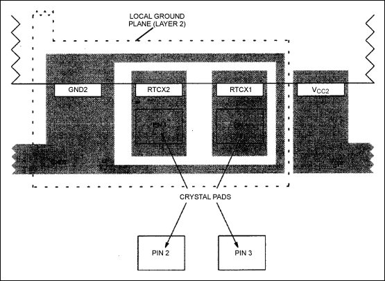
Because the crystal pins are highly susceptible to coupling noise, care must be taken when locating the external crystal on the PCB and when routing traces. The following guidelines are presented to reduce the effect of external noise on the RTC.
- Place the crystal as close as possible to the RTCX1 and RTCX2 pins. Short traces reduce stray capacitance and noise coupling.
- Keep the use small crystal bond pads and short traces to the RTCX1 and RTCX2 pins. Larger pads and longer traces are more likely to couple noise from adjacent circuits.
- Place a ground guard ring around the crystal. This helps isolate the crystal from adjacent signals
- Avoid routing signals beneath the crystal or RTCX1/RTCX2 traces. This helps isolate the crystal from adjacent signals. It is especially important to keep high frequency signals and devices as far away from the crystal as possible.
- Place a local ground plane directly beneath the ground guard ring. This helps isolate the crystal from signal layers below the crystal.

Figure 2. Example crystal placement on PC board.
 電子發(fā)燒友App

















評論