The Spartan?-6 family provides leading system integration capabilities with the lowest total cost for high-volume applications. The thirteen-member family delivers expanded densities ranging from 3,840 to 147,443 logic cells, with half the power consumption of previous Spartan families, and faster, more comprehensive connectivity. Built on a mature 45 nm low-power copper process technology that delivers the optimal balance of cost, power, and performance, the Spartan-6 family offers a new, more efficient, dual-register 6-input lookup table (LUT) logic and a rich selection of built-in system-level blocks. These include 18 Kb (2 x 9 Kb) block RAMs, second generation DSP48A1 slices, SDRAM memory controllers, enhanced mixed-mode clock management blocks, SelectIO? technology, poweroptimized high-speed serial transceiver blocks, PCI Express? compatible Endpoint blocks, advanced system-level power management modes, auto-detect configuration options, and enhanced IP security with AES and Device DNA protection. These features provide a lowcost programmable alternative to custom ASIC products with unprecedented ease of use. Spartan-6 FPGAs offer the best solution for high-volume logic designs, consumer-oriented DSP designs, and cost-sensitive embedded applications. Spartan-6 FPGAs are the programmable silicon foundation for Targeted Design Platforms that deliver integrated software and hardware components that enable designers to focus on innovation as soon as their development cycle begins.
Spartan-6 FPGA主要特性:
? Spartan-6 Family:
? Spartan-6 LX FPGA: Logic optimized
? Spartan-6 LXT FPGA: High-speed serial connectivity
? Designed for low cost
? Multiple efficient integrated blocks
? Optimized selection of I/O standards
? Staggered pads
? High-volume plastic wire-bonded packages
? Low static and dynamic power
? 45 nm process optimized for cost and low power
? Hibernate power-down mode for zero power
? Suspend mode maintains state and configuration with multi-pin wake-up, control enhancement
? Lower-power 1.0V core voltage (LX FPGAs, -1L only)
? High performance 1.2V core voltage (LX and LXT FPGAs, -2, -3, and -4 speed grades)
? Multi-voltage, multi-standard SelectIO? interface banks
? Up to 1,050 Mb/s data transfer rate per differential I/O
? Selectable output drive, up to 24 mA per pin
? 3.3V to 1.2V I/O standards and protocols
? Low-cost HSTL and SSTL memory interfaces
? Hot swap compliance
? Adjustable I/O slew rates to improve signal integrity
? High-speed GTP serial transceivers in the LXT FPGAs
? Up to 3.125 Gb/s
? High-speed interfaces including: Serial ATA, Aurora,1G Ethernet, PCI Express, OBSAI, CPRI, EPON, GPON, DisplayPort, and XAUI
? Integrated Endpoint block for PCI Express designs (LXT)
? Low-cost PCI? technology support compatible with the 33 MHz, 32- and 64-bit specification.
? Efficient DSP48A1 slices
? High-performance arithmetic and signal processing
? Fast 18 x 18 multiplier and 48-bit accumulator
? Pipelining and cascading capability
? Pre-adder to assist filter applications
? Integrated Memory Controller blocks
? DDR, DDR2, DDR3, and LPDDR support
? Data rates up to 800 Mb/s (12.8 Gb/s peak bandwidth)
? Multi-port bus structure with independent FIFO to reduce design timing issues
? Abundant logic resources with increased logic capacity
? Optional shift register or distributed RAM support
? Efficient 6-input LUTs improve performance and minimize power
? LUT with dual flip-flops for pipeline centric applications
? Block RAM with a wide range of granularity
? Fast block RAM with byte write enable
? 18 Kb blocks that can be optionally programmed as two independent 9 Kb block RAMs
? Clock Management Tile (CMT) for enhanced performance
? Low noise, flexible clocking
? Digital Clock Managers (DCMs) eliminate clock skew and duty cycle distortion
? Phase-Locked Loops (PLLs) for low-jitter clocking
? Frequency synthesis with simultaneous multiplication, division, and phase shifting
? Sixteen low-skew global clock networks
? Simplified configuration, supports low-cost standards
? 2-pin auto-detect configuration
? Broad third-party SPI (up to x4) and NOR flash support
? Feature rich Xilinx Platform Flash with JTAG
? MultiBoot support for remote upgrade with multiple bitstreams, using watchdog protection
? Enhanced security for design protection
? Unique Device DNA identifier for design authentication
? AES bitstream encryption in the larger devices
? Faster embedded processing with enhanced, low cost, MicroBlaze? soft processor
? Industry-leading IP and reference designs
Spartan-6 FPGA系列特性表:

Spartan?-6 FPGA應(yīng)用:

In-Car Infotainment System
Serving as a companion to the host processor, a single Spartan-6 LX45T FPGA supports audio/video acceleration, graphics subsystem, and vehicle networking functions.
圖1.汽車娛樂系統(tǒng)

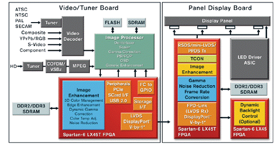
High-Resolution Video Flat-Panel Display with Dynamic Backlight Control Achieve higher image quality while reducing power and cost using Spartan-6 FPGAs withintegrated serial I/O capabilities.
圖2.帶動態(tài)背光控制的高清視頻平板顯示器系統(tǒng)

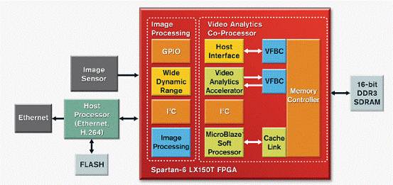
Surveillance Image Capture and Analytics Engine Integrate sensor interfacing, video analytics, image enhancement and network interfacing in a single Spartan-6 LX150T FPGA.
圖3.監(jiān)視圖像捕捉和分析引擎系統(tǒng)
Spartan?-6 FPGA SP605評估板
The Spartan?-6 FPGA SP605 Evaluation Kit conveniently delivers all the basic components for developing broadcast, wireless communications, automotive, and other cost- and power-sensitive applications that require transceiver capabilities in one ackage. Along with the evaluation board, cables, and documentation, the SP605 Evaluation Kit provides an integration of hardware, software, intellectual property (IP), and pre-verified reference designs so development can begin right out of the box.
The SP605 Evaluation Kit provides a flexible environment for higher-level system design, including applications that implement features such as high-speed serial transceivers, PCI Express?, DVI, and/or DDR3. The SP605 evaluation board includes an industry-standard FPGA Mezzanine Card (FMC) connector for scaling and customizing to specific applications and markets. The integration of Xilinx development tools help streamline the creation of systems that adhere to complex requirements.
This guide provides steps to setup the SP605 hardware and run a diagnostic demonstration that exercises a number of basic board features. It introduces a more complex Base Reference Design that exercises key features of the Spartan-6 FPGA. This guide also provides steps for installing the Xilinx? ISE? Design Suite: Logic Edition software, obtaining updates, and generating a license.
SP605評估板包括:
? Spartan-6 FPGA SP605 Evaluation Board
? ISE Design Suite Logic Edition: (device-locked) for Spartan-6 LX45T FPGA
? Includes ChipScope? Pro software and the ChipScope Pro Serial I/O Toolkit
? Includes PlanAhead? Design Analysis Tool
? Timing Driven Place and Route, SmartGuide?, and SmartXplorer Technology
? Documentation
? Hardware Setup Guide
? Getting Started Guide
? Hardware User Guide
? Reference Design User Guide
? Schematics and PCB files
? Universal 12V power supply
? Cables
? (2) USB
? Ethernet
? DVI to VGA adapter
? Reference Designs and Demonstrations
? Board Diagnostic Demonstration
? Base Reference Design featuring DSP48, Ethernet, memory, and serial transceiver integration
? MultiBoot Reference Design, featuring fail-safe configuration
? Integrated Memory Controller Reference Design
? Integrated Bit Error Ratio (IBERT) Reference Design
? PCIe? x1 Gen1 Reference Design
? Reference designs, demonstrations, documentation, and applications delivered on USB Flash drive to get started quickly
SP605評估板主要特性:
Spartan-6 FPGA
? XC6SLX45T-3FGG484 device
Configuration
? Onboard JTAG configuration circuitry
? 8 MB Quad SPI Flash
? 32 MB Parallel (BPI) Flash
? System ACE CF 2 GB CompactFlash (CF) card Memory
? 128 MB DDR3 Component Memory
? 32 MB Parallel (BPI) Flash (Also available for configuration)
? 8 Kb IIC EEPROM
? 128 MB Quad SPI Flash (Also available for configuration) Communications and Networking
? 10/100/1000 Tri-Speed Ethernet
? SFP transceiver connector
? GTP port (TX, RX) with four SMA connectors
? USB To UART bridge
? PCI Express x1 edge connector Expansion Connectors
? FMC LPC connector (1 GTP transceiver, 68 single-ended or 34 differential userdefined
signals)
? User GPIO with two SMA connectors
? 4 user I/O (1 x 6 header) Clocking
? 200 MHz oscillator (differential)
? 27 MHz Socketed oscillator (single-ended)
? SMA connectors for external clock (differential)
? GTP reference clock port with two SMA connectors Display
? Video - DVI / VGA
? 16 x 2 LCD character display
? 4 LEDs Control
? 4 Pushbuttons
? 4 DIP switches Power
? 12V wall adapter or ATX
? Voltage and current measurement capability of 2.5V, 1.5V, and 1.2V supplies

圖4.Spartan?-6 FPGA SP605評估板外形圖

圖5.Spartan?-6 FPGA SP605評估板方框圖和外設(shè)

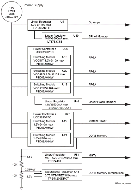
圖6. SP605評估板板載電源穩(wěn)壓器框圖
 電子發(fā)燒友App


評論