Battery-operated equipment is prone to the consequences of batteries installed backward, accidental short circuits, and other types of careless use. The effects of a reversed battery are critical. Unfortunately, it is difficult to guard against this situation.
To make equipment resistant to batteries installed backward, you must design either a mechanical block to the reverse installation or an electrical safeguard that prevents ill effects when the reverse installation occurs. Mechanical protection can be a one-way connector that accepts the battery only when oriented with the correct polarity.
For example, 9V radio batteries have mechanically dissimilar terminals, although a user fumbling with the mechanical connection can still momentarily make the reverse electrical connection. On the other hand, you can configure connectors for rechargeable battery packs so that momentary reverse connections are impossible unless the user modifies the connector.
The greatest challenge, however, is in applications powered by one or more single-cell batteries such as AA-alkaline, NiCd, and nickel-metal-hydride types. In general, these batteries offer no mechanical means for preventing the reversal of one or more cells. For these systems, a designer must ensure that any flow of reverse current is low enough to avoid damaging the circuit or the battery. A variety of circuits can provide this assurance.
Diodes Provide the Simplest Protection
The simplest form of battery-reversal protection is a diode in series with the positive supply line (Figure 1a). The diode allows current from a correctly installed battery to flow to the load and blocks current flow to a backward-installed battery. This solution has two major drawbacks: The diode must handle the full load current, and its forward voltage drop shortens the equipment's operating time. (The regulator output is one diode drop below the battery voltage, so the regulator drops out prematurely.)If the application calls for an alkaline or other type of battery with relatively high output impedance, you can guard against reverse installations using a parallel (shunt) diode. The circuit in Figure 1b is simple but far from ideal. This approach protects the load yet draws high current from the shorted battery. As before, the diode must be able to handle the high current.
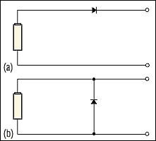
Figure 1. The simplest protection against reversed-battery current is a series (a) or shunt (b) diode.
As an improved battery-reversal measure, you can add a pnp transistor as a high-side switch between the battery and the load (Figure 2a). When you install the battery correctly, the current-limiting resistor in the base lead forward-biases the base-emitter junction. A backward-installed battery reverse-biases the transistor, and no current can flow. This arrangement is better than the series diode, because the saturated pnp transistor offers a lower voltage drop than most diodes and thereby improves operating efficiency by lowering the power dissipation.
Check for Drawbacks
The lower voltage drop of pnp transistors also extends operating time, because it allows the battery voltage to discharge to a lower level. These transistors offer low cost and a low saturation voltage, but they also have drawbacks. For instance, base current dissipates part of the battery's useful energy as VIN × IB, and the beta (approximately 50 maximum) of most power pnp transistors demands substantial base current for a given load current.You must design for a base current that is adequate for the combination of maximum load and minimum VIN. This fixes the value of base current and then causes lower efficiency at lighter loads, unless you provide sophisticated circuitry to modulate the base current as a function of load current. These criteria also apply to the use of an npn switch between the load and the battery return (Figure 2b) but with one major difference: Power npn transistors' much higher betas lower their base-current loss for a given load current.
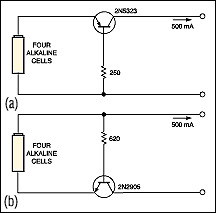
Figure 2. Because its forward drop is lower, a high-side pnp transistor (a) offers better reverse-current protection than does a diode. Better yet is a low-side npn transistor (b) whose higher beta means a lower base current and lower power loss.
Replace Bipolar Transistors with MOSFETs
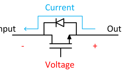
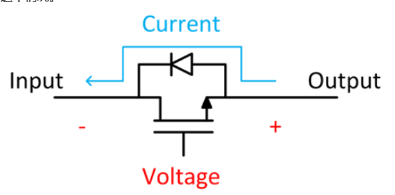
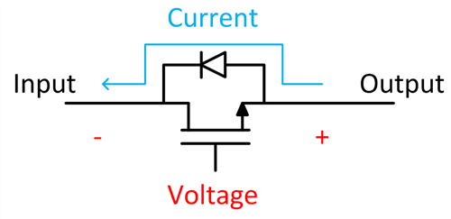
For a given load current, the low resistance of a fully enhanced MOSFET drops much less voltage than that of an equivalent bipolar transistor. The result is lower power dissipation, which enables the MOSFET to handle much higher load currents than are possible with a bipolar transistor of the same size. This advantage has led to the manufacture of n- and p-channel, logic-level MOSFETs for operation at 5V and 3V and even lower supply voltages. NMOS FETs include the Motorola MTP-3055EL, the Harris RFD14N05L, and the Siliconix Si9410DY. Examples of PMOS FETs are the Siliconix Si9433DY and Si9434DY and the National Semiconductor NDS9435.Pay careful attention to a MOSFET's orientation in the circuit. MOSFETs have an intrinsic body diode that conducts current under forward-bias conditions. This current flows from the drain to the source for a PMOS FET and from the source to the drain for an NMOS FET. Whether using an NMOS or a PMOS FET as a low- or high-side switch, orient the device's body diode in the direction of normal current flow. Then, a reversed battery reverse-biases the diode and blocks the flow of current.
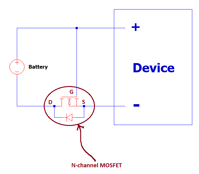
NMOS FETs are more attractive than PMOS FETs for high-current applications, because NMOS FETs offer lower on-resistance than PMOS counterparts of the same size. Because you must pull the gate voltage of an NMOS FET above the source for full enhancement, an NMOS FET belongs in the battery-return path (Figure 3). Thus, if you install the battery correctly, battery voltages higher than 10V (5V for logic-level MOSFETs) fully turn on the MOSFET. Reversing the battery pulls the gate terminal low and turns off the MOSFET.
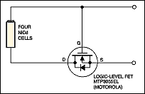
Figure 3. A low-side logic-level NMOS FET for reverse-current protection handles more current than an equivalent bipolar transistor.
A low-side switch has one drawback: Ground-return currents flowing through the switch produce small voltage drops that can interfere with circuit operation. The alternative is a high-side switch. However, using an NMOS FET as a high-side switch still requires a gate drive in excess of the source voltage, that is, a gate drive higher than the battery voltage. Figure 4 shows one solution in which a charge-pump device (IC1) boosts the gate voltage well above the source. This circuit fully enhances the MOSFET when the battery is installed correctly.
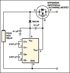
Figure 4. To provide reverse-current protection without disrupting ground-return currents, add a high-side NMOS FET driven by a charge-pump IC.
In Figure 4, IC1 accepts battery voltages of 3.5V to 16.5V and regulates the battery's output to (VBATT+10V). This circuit allows standard, enhancement-mode, NMOS FETs to operate from battery voltages as low as 3.5V. Because the charge pump runs on the battery voltage and thus also needs protection from battery reversal, the circuit connects a diode between the battery's positive terminal and the IC's VCC terminal.
PMOS FETs operate on the high side and require no extra circuitry for gate drive. However, the PMOS switch is generally twice as expensive and has nearly three times the on-resistance as an NMOS device of comparable power-handling capability operating with a similar drain-to-source voltage. You can enhance currently available PMOS transistors with 5V or even 3V of gate drive.
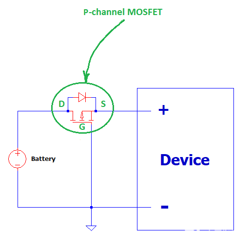
If your circuit's battery voltage is at least 10V, you can connect the gate of the PMOS FET directly to the battery return (Figure 5). As before, you must connect the transistor backward (with respect to normal practice) to orient its body diode in the direction of normal current flow. This connection applies the battery voltage between the gate and the drain, but the voltage between the gate and the source controls the channel resistance. The body diode, however, produces a source voltage one diode drop below the drain when you first apply VBATT. The result is a hard gate-source voltage equal to -(VBATT-VDIODE) that quickly enhances the FET, bringing the VDS drop to a desired minimum.
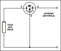
Figure 5. This high-side PMOS FET switch offers simple reverse-current protection in exchange for higher on-resistance and cost.
The Challenge of Low-Battery Voltages
For battery voltages lower than 10V but higher than 2.7V, you can use a low-voltage PMOS FET, such as the Siliconix Si9433DY or Si9435DY. Providing battery-reversal protection for battery voltages lower than 2.7V, on the other hand, can be a challenge. One solution is to use a bipolar transistor, which entails base-current losses. Another is the use of a low-threshold PMOS FET with a charge pump for driving the gate voltage below ground (Figure 6). This circuit can operate with 5V or 3.3V output voltages. Although specified for two-cell operation, the circuit typically starts with input voltages as low as 1.5V.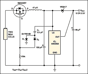
Figure 6. Using a high-side PMOS FET switch with low battery voltage requires a charge pump (D1, D2, and C1) to drive the gate voltage below ground.
One or two battery cells don't necessarily produce enough gate-source voltage to fully turn on the FET. However, the switching node of IC1's step-up DC/DC converter drives a simple charge pump, comprising C1, D1, and D2, that generates more than enough drive for that purpose. For VIN = 2V, the gate drive is approximately -(VIN+VOUT) = -7V.
A battery reversal makes the CMOS DC/DC converter resemble a forward-biased diode; the converter turns off the switch by hauling the gate voltage at least one diode drop above the source. The 100-kilohm pulldown resistor discharges the gate capacitance within 140msec yet loads the charge pump lightly and offers no interference with enhancing the MOSFET. Again, the circuit connects the MOSFET backward to prevent the FET's body diode from being forward-biased during a battery reversal.
You can also use an NMOS low-side switch for protection by using the DC/DC converter output to boost the gate voltage (Figure 7). When regulating normally, the converter (IC1) pulls the MOSFET's gate above its source. If you install the battery backward, the load resistance discharges the output-filter capacitor, which turns off the MOSFET by holding the gate and the source at the same potential.
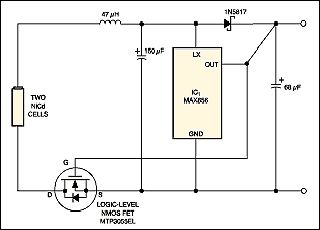
Figure 7. The output of IC1's boost converter drives this low-side NMOS FET switch.
On the other hand, if the load is light and you first install the battery correctly and then quickly reverse it, the output capacitor's charge holds the MOSFET on and allows reverse current to flow through the regulator. For the components shown, this condition persists for about 100msec while the capacitor discharges through the regulator. The MOSFET then turns off and blocks current flow thereafter.
A similar version of this article appeared in the March 1, 1996 issue of EDN.
 電子發(fā)燒友App










評(píng)論