Designing the external interface to an industrial or automotive application can be challenging for an uninitiated systems engineer. The bouncing of switch and relay contacts can produce arcs that threaten system reliability. Electrostatic discharge (ESD) can also threaten reliability and uptime. The purpose of this discussion is to ease the task of designing an interface between the inputs of a microcontroller and a hostile industrial or automotive environment.
Switch Bounce
The ideal switch operation depicted in most textbooks—a single transition that occurs instantly on actuation, followed by zero on-resistance—has never existed! Real switches exhibit a finite resistance called "contact resistance," that increases over time with the number of switch actuations. Contact resistance for a new switch ranges from less than 50mΩ to 100mΩ, depending on the contact material, power loading, environmental conditions, and switch usage.As a switch changes state, its contacts travel through several open-close cycles called "contact bounce" before coming to rest in the final state. In some cases, this rapid contact bounce produces a changing resistance as the moving contact wipes across the stationary contact. In Figure 1, a pushbutton switch supplies 24V (a typical industrial-control voltage) to the resistor. Notice that at least four major switching transitions occur before the output comes to rest at 24V. To a digital control system, these transitions could be interpreted as four separate contact closures.
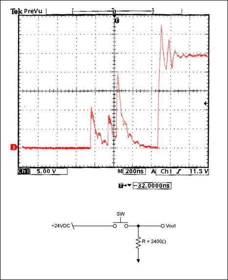
Figure 1. Switch contact bounce and test circuit.
Contact bounce is not acceptable, because automotive- and industrial-control systems require accurate, real-time data in the form of definite state changes. (For more information on switch bounce and related issues, see the application note, "Switch Bounce and Other Dirty Little Secrets.") Factors that affect the rated capacity of a switch include the power factor, AC or DC voltage, voltage amplitude, type of load (lamp or motor; that is, whether the load is resistive, inductive, or capacitive), and the magnitude of current through the switch. Typically, the AC-voltage rating for a switch is specified at a given current level and power factor. Its operating voltage must be less than this AC-voltage rating.
The type of load on a switch affects its rating drastically. A resistive load such as a tungsten heater is the least stressful. Inductive loads and motor loads both place additional stress on the switch as it opens and closes. The bouncing switch contacts can encounter inrush currents 3 to 10 times' greater than steady-state levels. Bounce occurs during both opening and closing, and the resultant arcing causes contact wear, higher resistance, and lower reliability.
Lamp and capacitive loads represent the worst case. At the instant of switch closure, both of these loads subject the switch to a short circuit. A lamp's cold resistance is close to 0Ω, and a discharged capacitor is a short circuit at the instant voltage is applied! This state change can produce inrush currents up to 100 times the steady-state value. To compound the problem, switch contacts are bouncing during this short-circuit interval. High current levels and bouncing contacts produce severe arcing across the switch contacts that causes contact erosion. What's worse is that repeated cycles of switch operation with severe arcing can create a short circuit by welding (fusing) the contacts together.
Last to be considered when specifying a switch for automotive or industrial environments are power level and contact material. Silver contacts are usually specified for power levels above 0.4VA (the power-level range or wet-contact rating). This power level allows enough arcing to remove any silver tarnish (oxidation that increases the contact resistance). Thus, minimal arcing is beneficial, but the excessive arcing caused by a lamp or capacitive load destroys the switch contacts.
For power levels below 0.4VA (the low-level range or dry-contact rating), gold-plated contacts should be used. Because these power levels lack sufficient energy to cause arcing, silver contacts become encrusted with contact oxide (an insulating material) and therefore fail to close the circuit. Plating the silver contacts with gold, however, prevents tarnish and thereby extends the contact life to that of its mechanical life rating. Also usable for the low-level range (in place of domed contacts) are bifurcated contacts, that is, two-pronged parallel switch contacts. The two prongs provide a wiping action that maintains reliability by helping to remove the contact tarnish.
To avoid signal degradation due to contact wear, you should not route signals through switch contacts that also perform power-level control (meaning contacts that control motors, lamps, or solenoids). In addition, any contacts providing signals to a microcontroller or industrial control system must incorporate signal debouncing through hardware or software.
With design cycles now measured in months instead of years, it has become a serious problem to discover midway through a project that your microcontroller is not operating in real time because its internal resources (timers, RAM, interrupts, and even polling to debounce inputs) are stretched beyond capacity. You need a solution that reduces the total system cost, places minimal dependence on the microcontroller (software and RAM), requires little PC-board space, and contributes to system reliability.
As demonstrated in Figure 1, a simple pulldown resistor is not enough to enable a switch to make a clean and definite state change. Figure 2 illustrates a typical textbook solution to the switch-bouncing problem. Two resistors and two logic NOR gates form an R-S latch (Figure 2a). The two resistors pull down the R or S input when the switch is open, and they limit the flow of current to ground if the switch contacts should fuse. A truth table for the R-S latch illustrates its operation (Table 1).
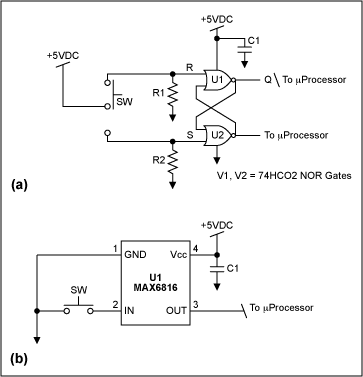
Figure 2. Single-switch R-S latch CMOS switch-debouncer circuit (a) and single-switch CMOS switch-debouncer circuit (b).
Table 1. R-S Latch Switch Debouncer
|
|
|
|
|
|
|
|
|
|
|
|
|
|
|
|
|
|
|
|
The Q output is logic high when the switch is set to S. Thus, contact bounce simply causes a logic low at the S input. This input is a holding state, because the pulldown resistor at R holds that input at logic low. The converse holds when the switch is set to the R position: Q is at logic 0, and it maintains a holding state in the presence of contact bounce. This circuit is acceptable, but it requires two extra NOR gates. Thus, there is room for improvement.
One disadvantage of this debouncer circuit is the single-pole double-throw (SPDT) switch required, which costs more than a single-pole single-throw (SPST) switch and is physically larger. The larger switch, resistors, and NOR gates necessitate more PC-board space. Furthermore, the truth table's "unstable state" indicates that the state of Q cannot be guaranteed when both inputs are logic high simultaneously. This condition can easily occur when troubleshooting in the field, if, for instance, the low and high inputs are shorted by a meter lead.
Make-before-break switch contacts allow unstable states to occur, so the contacts for this circuit must be rated break-before-make. Because the circuit does not provide voltage-level shifting, three wires must be run to the switch. The additional circuitry and PC-board space increase system costs.
A new debouncing technique employs a switch-debouncer IC to reduce the component count, the power consumption, and the PC-board space (Figure 2b). U1 is a CMOS switch debouncer connected directly to a SPST switch. Its input has a 63kΩ pullup resistor for logic-high inputs, which saves PC-board space. Capacitor C1 decouples the VCC pin. Closing the switch pulls the IN pin low and provides a logic low at the OUT pin. The OUT pin does not change state until the IN pin is stable for 40ms, which hides the effect of any contact bounce.
A not-so-obvious advantage of this circuit is resistive loading of the switch by the internal 63kΩ resistor, ensuring reliability and an indefinite switch life. Disallowed states do not exist in this circuit, because the input is either low or high. Moreover, the IC's undervoltage-lockout circuitry ensures a condition crucial in automotive and industrial applications: that the OUT pin be in a known state during power-up. The circuit improves reliability and lowers system costs by requiring fewer components, a less expensive SPST switch, and only two wires connected to the switch.
Relay Bounce
Relays are also represented as ideal switching devices in textbooks. Like the switching contacts of an ideal switch, those of a relay are assumed to have zero resistance and a single switching transition that occurs immediately on actuation. As with switches, actual relay contacts, of course, have contact resistance, which increases over time with repeated actuations. Typical contact resistance ranges from less than 50mΩ to 200mΩ when new.The actuation of a relay is also mechanical. Unlike the switch, however, a SPST relay has only one movable contact, which connects electrically by a wire to one of the external-contact terminals. The stationary contact connects to the other external contact. Relay contacts also make several open-close cycles of contact bounce before coming to rest in the final state. This contact-bounce interval is in addition to the relay's operate and release times, which can measure tens of milliseconds.
Figure 3 shows the voltage across a resistive load after actuating an industrial relay that supplies 24V to the resistor. At least 12 major switching transitions are evident before the contacts come to rest at 24V. An automotive microcontroller or industrial control system would interpret these transitions as multiple cycles of the relay contacts.
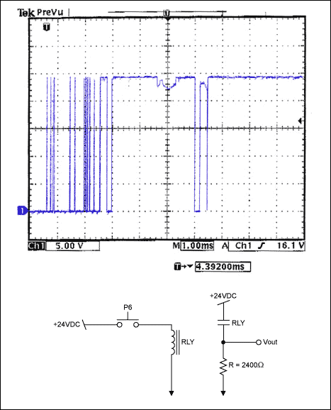
Figure 3. Relay contact bounce and test circuit.
As for switches, the worst-case loads for a relay are lamp and capacitive loads. These loads subject the contacts to additional stress by creating a short circuit at the instant the relay contacts open or close. You should therefore specify the contacts of a relay for the type of load expected in the application. Unlike switch contacts, relay contacts are rated by their AC/DC resistive-load and "contact-horsepower" capabilities.
The contact-horsepower rating provides the maximum motor loading to which a relay can be subjected without premature failure. Relays used in industrial- and automotive-control systems for the purpose of isolating one power source or ground from another are subject to the same "dry" and "low-level" ranges of power dissipation. Gold-plated or bifurcated relay contacts must be specified for signal-power levels under 0.4VA. Using a power-level relay with silver contacts means the designer can expect field failures soon!
Contact bounce with high-level current flow subjects relay contacts to the type of contact failure seen in switches. Again, signals should not be derived from contacts that power motors, solenoids, or similar components in an automotive- or industrial-control system. A separate set of contacts should be used for that purpose.
As signal translators, the relay and resistor are not adequate for providing a clean signal to a microcontroller or control system. Figure 4 shows a textbook debouncer applied to relay contacts for a system microcontroller.[7] A process sensor, such as a remote pressure switch, actuates the relay (mounted on the control board) with 24VDC. The value of the RC lowpass filter should be large enough (20ms to 200ms) to mask any bounce time introduced by the relay contacts.
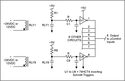
Figure 4. Eight-bit debouncer circuit for a microcontroller.
As the capacitor charges and discharges, the Schmitt-trigger IC provides output changes with hysteresis and a sharp, definite switching transition. This circuit requires polling software, and its high parts count calls for more PC-board space (for a typical 8-bit input module, it includes two 74HC14 Schmitt-trigger ICs, eight capacitors, and 16 resistors).
Listing 1 is a pseudo-port-polling subroutine that monitors a relay in the above circuit for changes in the contact state. For each pass through the main loop, the main program jumps to the Check_Port subroutine, reads input data, and stores it in the Port1 memory location. It compares Port1 data with old port data in the Port_P memory location and performs a bit test at line 4. If no input bits have changed since the last reading of Port1 (Port_P contains previous data), the program execution exits this subroutine and continues again at the main program. If bits have changed, it adds "1" to the Count memory location. Count is compared with the constant "N_Pass_Value" (number of passes through the main program before the relay is assumed debounced), and if the Count value is less than N_Pass_Value, execution returns to the main program again. If Count equals N_Pass_Value, Count is set to zero, the new Port1 data is copied into Port_P, and execution passes from the subroutine back to the main program.
Listing 1. Subroutine for Pseudo Polling Code
- Check_Port: Read Port Data
- Store Port_Data in Port1
- Compare Port1 with Port_P (EX-OR Port1 with Port_P)
- Test for Bit Changes: (No) Return from Check_Port subroutine, (Yes) Continue
- Add 1 to Count
- Count = N_Pass_Value: (No) Return from Check_Port subroutine, (Yes) Continue
- Set Count = 0
- Store Port1 in Port_P
- {Do something with the new port data}
- Return from Check_Port subroutine with new Port_P data for main program
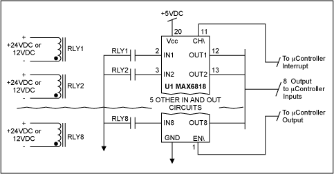
Figure 5. Eight-bit CMOS switch-debouncer circuit for a microcontroller.
Listing 2 shows a pseudo code-interrupt service subroutine for the circuit in Figure 5. Listing 2 does not appear to have an advantage over Listing 1 in code length, but its advantage is significant for processing input data in real time, as required in automotive and industrial applications. Most importantly, the interrupt-service routine runs only when new data is available (when the relay or switch changes state). This action allows the processor to perform other time-intensive routines and handle the data closer to real time.
Listing 2. Subroutine for Pseudo Interrupt Code
- New_Port: Set EN\ pin bit low
- Read Port Data
- Store Port_Data in Port_P
- Set EN\ pin bit high (Reset CH\ = High)
- Return from Check_Port service subroutine with new Port_P data ready for main program
- Main_P: Continue program prior to interrupt
- {Do something with the new port data when required}
Figure 6 and Listing 3 show a pseudo-polling-debouncing routine that checks for changes in the state of the relay contacts, with minimal use of hardware, resistors, or excessive software. The resistors pull down the microcontroller input pins when the relay contacts are open. R is chosen for the type of relay contacts specified by the designer, considering the contact material and load current. The subroutine DB_Check_Port (Listing 3) functions as follows.
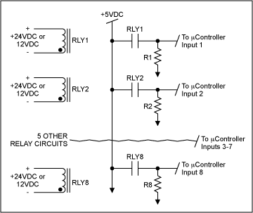
Figure 6. Minimal-component relay interface for a microcontroller.
Program execution jumps to this subroutine during each pass through the main program. It reads input data and stores it in the Port1 memory location, for comparison with old port data in the Port_P memory location (lines 1 through 3). The code at line 4 performs a bit test. If no bits have changed since the last reading of Port1, execution exits the subroutine and continues at the main program (Port_P contains previous data). When bits have changed state, a timer/counter loop (lines 6 and 7) marks 50ms by ticking away CPU clock cycles. After that interval expires, Port1 data is transferred to the Port_P memory location for use by the main program.
This approach has two main problems: It wastes CPU time, and it provides no electrostatic-discharge (ESD) or transient protection on the input lines. Slowing down the data-processing time for a timer/counter loop is not acceptable in automotive and industrial applications, where sensor and system-control signals must be handled in real time. Furthermore, this design provides no input protection for the microcontroller pins, because the pins connect directly to the relay terminals. The microcontroller's integrity can be easily compromised by a technician replacing a relay, because that action can allow ESD directly into the microprocessor pins.
Listing 3. Subroutine for Pseudo Timer/Counter Debouncing Code
- DB_Check_Port: Read Port Data
- Store Port_Data in Port1
- Compare Port1 with Port_P (EX-OR Port1 with Port_P)
- Test for Bit Changes: (No) Return from Check_Port subroutine, (Yes) Continue
- Store 50ms_Count in Counter
- DB_TMR: Decrement Counter by 1
- Test Counter = 0: (No) Go to DB_TMR, (Yes) Continue
- Store Port_Data in Port_P
- {Do something with the new port data}
- Return from Check_Port subroutine with new Port_P data for main program
Automotive Specifics
Without exception, automotive environments present a challenge to the design engineer. Automotive systems must survive temperatures that range from -40°C to +70°C, continuous mechanical vibration, and contaminants such as lubricants, coolants, and other liquids. Static overvoltages and reverse voltages, switching spikes, transients from parallel and series loads, low-voltage noise transients, and load dumps will be discussed.You must consider the possibility of static overvoltage or reverse-polarity voltage from the vehicle's battery system. The vehicle power rail carries voltages as high as +24V when jump-starting a dead battery. A microcontroller's power supply must be capable of withstanding this voltage, as must any input that can be short-circuited by a component failure or the action of a service technician. If a vehicle battery is inadvertently connected in reverse, all systems connected to the vehicle's power rail will be exposed to negative voltage. Referring again to Figures 2b and 5, protection on the debouncer inputs of the MAX6816, MAX1617, and MAX6818 can handle ±25V (a logic high of +25V and a logic low of -25V).
As an alternative, you can protect each input by installing a series resistor and back-to-back zener diodes (or transient voltage suppression, or TVS, diodes) in parallel with the pulldown resistor (Figure 2a). For further protection, the microcontroller's power supply should also include a reverse-protection diode in series with its input. When parallel-connected inductive loads such as fuel pumps, relays, horns, solenoids, and starter motors are disconnected (turned off), they can generate negative-voltage transients as high as -100V on the power rail.
Similarly, positive-voltage transients up to +100V can be developed when a series-connected load such as a switch in the rear of the vehicle is disconnected from an inductive component like a long wiring harness that supplies +12V to the rear of the vehicle. The wiring harness in a vehicle contains distributed capacitance and inductance that can superimpose ±100V switching spikes on the vehicle's +12V power rail. ESD and transient-input protection is a must in this environment.
When the low impedance of an engine's starter motor is cranking the engine over, the resulting heavy current can produce low-voltage noise transients by momentarily depressing the +12V power rail to levels as low as +5V. This problem is especially troublesome during cold weather when the oil viscosity is higher. Moreover, the starter motor's rotational speed during starting is not continuous but varies due to the effect of mechanical components attached to the crankshaft. The result is a variation of level in the low-voltage transient. The system controls (electronic modules) being designed should therefore have sufficient "carry-over" capacity (power-supply input capacitance) to allow operation during these low-voltage transients. One advantage of circuit integration and fewer components is less power dissipation, which allows a smaller carry-over capacity.
The last hazard to consider is load dumps, which occur when an air-conditioning clutch, flashing headlamps, or other large load is suddenly disconnected from the power rail. If the engine is accelerating or running at high speed, the alternator's field-excitation circuit (whose time constant is 40ns to 400ms) can subject the power rail to voltages between +10V and +120V.
A designer must consider all of the above when developing a control system for the automotive environment. Figure 7 shows a simple view of the various loads connected to a power rail, with their associated distributed inductance, capacitance, and resistance. Connecting a switch that simply signals an event, like an alarm door switch or a transmission shift-point pressure switch, exposes the controller input to all the transient hazards mentioned above.
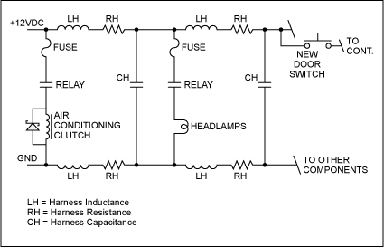
Figure 7. Vehicle wiring-harness model.
Input protection for a typical HCMOS device connected to the power rail is illustrated in Figure 8a. Resistors R1 and R3 are chosen to limit current through the switches when they are closed (dry- or wet-contact conditions) and to pull the inputs up to +12V. Capacitors C1 and C3 (typically small, 22nF to 100nF, ceramic capacitors) decouple to ground any radio-frequency interference from sources such as the ignition system and CB radios. Resistors R2 and R4 limit currents to the HCMOS inputs during a worst-case transient voltage of +150V. Finally, capacitors C2 and C4 in conjunction with R2 and R4 form an RC debouncer for the input, providing a typical time constant of 50ms to 200ms.
Another alternative employs an IC (MAX6817) that includes two ESD-protected debouncers in a SOT-23 surface-mount package (Figure 8b). At first glance, the transient protection of Figure 8a appears to be missing, but that protection is not required for the MAX6817 inputs. Resistors R1 and R3 are not needed, because U1 includes a 63kΩ resistor. Capacitors C1 and C3 are optional, and typically not required because the input protection is internal to U1. Resistors built into the MAX6817 IC (U1) limit input currents.
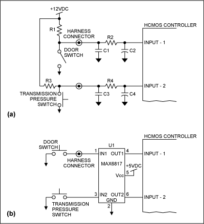
Figure 8. Discrete-component, HCMOS input-protection and debounce-interface circuit (a) and single-IC, HCMOS input-protection and debouncer-interface circuit (b).
Finally, the RC debouncer combination of C2 and C4 with R2 and R4 is not required, because U1 debounces signals for at least 40ms after the contact bounce has settled. U1's extremely low supply current (6μA, typ) allows the system to handle low-voltage noise transients with less holdup capacity. The Figure 8b circuit also provides undervoltage lockout for protection when the vehicle battery is disconnected or reconnected.
The mechanical shock waves that are transformed into electrical signals from pressure switches and other transducers are often overlooked by electronics designers but are of concern to automotive engineers. For example, a pressure switch monitors the hydraulic fluid in an automatic transmission during acceleration, both to indicate the appropriate shift point for the transmission and to send a signal to the engine controller (microcontroller).
Because this fluid pressure does not change instantaneously (nor does voltage on a capacitor or current through an inductor), the pressure output includes overshoot and ringing at the shift point. Thus, the pressure-switch signal requires debouncing not only for contact bounce in the pressure switch but also to debounce the mechanical shock wave. Switches that monitor coolant pressure also call for debouncing (because air in the engine coolant causes cavitation), and temperature switches require debouncing to mask mechanical and electrical effects. These mechanical-shock issues also arise in industrial applications.
Appendix: ESD Protection
Studies have shown that ESD accounts for 10% to 30% of all failures. Although many excellent books discuss ESD in detail, this appendix offers only a brief glimpse into that complex world.A surface can easily gain electrons (negative charge) or lose electrons (positive charge) when two different materials come in contact and are rubbed together. Triboelectrification (rubbing) causes electrons to collect in pools on nonconductive surfaces, because for voltages under 2kV the electrons cannot go through or over a nonconductive surface. Such pools form positive or negative electrostatic fields, producing voltage gradients between the surfaces with a force field that can pull or push the charges.
The fields near these pools are intense, but the charges (electrons) prefer to disperse over and through a conductive surface. John M. Kolyer provides the analogy of a pool of water with an extremely thin dam erected across the center. If water (electrons) is added to one side, that side exerts a force toward the lower pool perpendicular to the dam, causing the dam to eventually break (ESD discharge) and allow water (electron flow) into the lower pool (conductive surface). This analogy and the concept of electrons in pools holds for voltages under 2kV. Because a voltage gradient of 100V typically destroys MOSFET gates, our low-cost, minimal resistor count, software-debounce circuit definitely leaves a system at risk for ESD damage to the microcontroller!
Voltages above 3kV are considered high-voltage ESD, for which the concept of a pool of electrons on a nonconductive surface no longer applies. At such higher voltages, the excess charge on a nonconductive surface easily ionizes the air and discharges (via a spark) to any nearby conductive surface. The spark allows current to flow from one surface to the other through the air. Lightning is an excellent example of this form of discharge. Sharp corners on a conductive surface at higher voltages tend to concentrate the E-field lines of force, which more easily ionizes the air in a corona discharge. For this condition at 10% to 20% relative humidity, the risk of ESD hazard runs very high.
Objects that generate static come in many forms. Rubbing two surfaces together (triboelectric charging) or peeling a piece of plastic tape from a PC board are two examples. Canned cryogenics of the type used for troubleshooting have been shown to generate charged droplets. Another example is the failure of high-voltage insulation in a vehicle's high-voltage spark system can develop voltages high enough to cause corona discharge between surfaces.
Prevention of ESD damage should consider environmental factors such as humidity (which reduces ESD but does not eliminate it). Conductive wrist straps and mats should be part of the ESD-safe workplace. Conductive materials should be grounded, and this applies especially to screwdrivers. (The screwdriver is a conductor with sharp corners, a nonconductive handle, and an ungrounded tip begging for ESD.)
Note that grounding is useless on nonconductive surfaces. Some type of ESD protection must therefore be included with circuits that might come in contact with ESD sources directly or indirectly. Conductive keypads alone will not provide protection if a service technician can possibly discharge his or her screwdriver into the input of a microcontroller.
TVS diodes and ICs can protect a system from ESD and transients. TVS diodes provide a low clamping voltage with no degradation of themselves. They are available from several manufacturers, with working voltages from +5V to +24V. When specifying leaded TVS diodes (that is, not surface-mount types), keep the leads as short as possible to eliminate lead inductance, which nulls the diode's benefit by increasing its response time.
The circuits in Figures 2b and 5 each provide ESD protection for the microcontroller inputs. MAX6816, MAX1617, and MAX6818 inputs can handle ±25V, and they are ESD-protected to +15kV. The ESD protection is provided during all states of normal operation, power up, power down, and shutdown. This type of ESD and input protection is ideal for automotive and industrial applications. The benefits of an ESD-protected debouncing IC include ESD protection and debouncing in the same package, thereby minimizing the PC-board area, reducing the parts count, and increasing the system's reliability and robustness.
Reliability and robustness have become central issues for the automotive designer, as vehicle manufacturers develop vehicles that steer and brake by "wire." Vehicles may soon have electric motors that provide power-assisted steering, braking by motors on each wheel, fuel throttles with motor-controlled acceleration, and more. All these innovations will require a larger wiring harness, yet the present harnesses are already subject to transient faults.
Bibliography
- "Technical Information," EAO World Class Switching Products, Catalog 102B, Nov. 1998, pp. 104-105.
- "Rerating Current," Design Guide 2000 NKK Switches, Catalog No. 9908, May 1999, p. Z3.
- Pasahow, Edward J., "An Introduction to Interfacing and Peripheral Equipment," Microprocessor Technology and Microcomputers, McGraw-Hill, 1988, p. 234.
- Katz, Randy H., "Practical Matters," Contemporary Logic Design.
- Prestopnik, Richard J., "Basic Input and Output Interfacing," Digital Electronics, Saunders College Publishing, 1990, pp. 465-466.
- "General Purpose PC Board Relays," Potter & Brumfield General Stock Catalog, Catalog No. 13C222, Aug. 1988, pp. 4-24.
- Horowitz, Paul, and Hill, Winfield, "Switch Bounce," The Art of Electronics, Cambridge University Press, 1994, pp. 576-577.
- Fryburg, George A., Stocker & Yale, "ESD-Safe Lighting," Robotics World, March/April 2000, pp. 36-38.
- Kolyer, John M. and Watson, Donald E., ESD From A to Z, International Thomson Publishing, 1996.
- "Automotive Applications," High-Speed CMOS Designer's Guide, Signetics/Philips, 1988, pp. 3-39 to 3-44.
- "Switch Bounce and Other Dirty Little Secrets," Maxim application note, Sept. 2000.
 電子發(fā)燒友App













評(píng)論