Overview
There are 16 physical ports (16 Tx and 16 Rx) or links that can be configured as either channelized or unchannelized in the DS31256. Channelized ports can handle one, two, or four T1 or E1 data links. The clock for these ports or links can support a gapped clock. This application note describes how to realize gapped clock applications in the DS31256, a 256-channel HDLC controller.Unchannelized Application with Gapped Clock
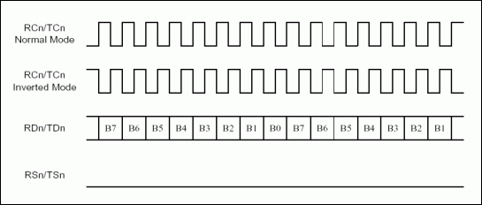
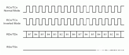
Figure 1. Unchannelized link timing with normal clock.
Figure 1 shows the timing relation of the clock RCn/TCn and data RDn/TDn of an unchannelized link without a gapped (i.e., normal) clock. The data is a contiguous serial stream with no concept of time slot. Every eight bits are grouped together into a byte with arbitrary alignment. The first bit received (B7) is the most significant bit (MSB) of an octet. The last bit received (B0) is the least significant bit (LSB). Bits that are to be processed by the DS31256 are clocked in or out on the rising or falling edge of RCn/TCn.
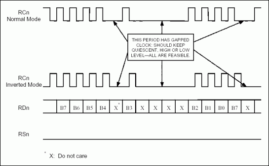
Figure 2. Unchannelized receive link timing with gapped clock.
Figure 2 shows the timing relation of the receive clock RCn and data RDn of an unchannelized link with gapped clock. The receive data is a contiguous serial stream with no concept of time slot. Every eight bits are grouped together into a byte with arbitrary alignment. The first bit received (B7) is the MSB of an octet. The last bit received (B0) is the LSB. Bits that are to be processed by DS31256 are clocked in on the rising or falling edge of RCn. Bits that should be ignored (denoted as X) are squelched by holding RCn quiescent. Figure 2 shows the quiescent period of RCn to be low. A high level, effected by extending the high phase of the previous valid bit, is also acceptable. Selection of bits for processing is arbitrary and is not subject to any byte alignment or frame boundary considerations.
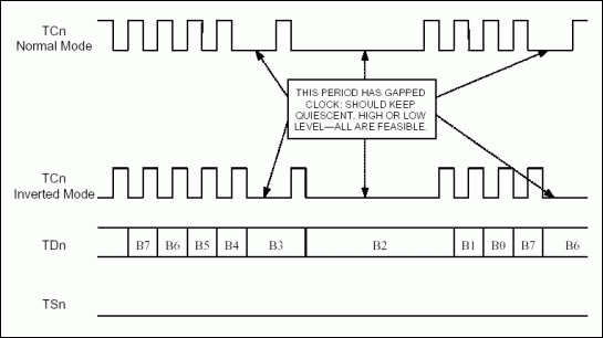
Figure 3. Unchannelized transmit link timing with gapped clock.
Figure 3 shows the timing relation of the transmit clock TCn and data TDn signals of an unchannelized link with gapped clock. The transmit data is a contiguous serial stream. There is no concept of time slot in an unchannelized link. Every eight bits are grouped together into a byte with arbitrary byte alignment. Octet data is transmitted, starting with the MSB (B7) and ending with the LSB (B0). Bits are updated on the rising or falling edge of TCn. A transmit link can be stalled by holding the corresponding TCn quiescent. In Figure 3, bits B3 and B6 are shown to be stalled for one cycle while bit B2 is shown to be stalled for three cycles. The quiescent period is shown to be low on TCn. A high level, effected by extending the high phase of the previous valid bit, is also acceptable. Gapping of TCn can occur arbitrarily without regard to byte nor frame boundaries.
Unchannelized Application with Gapped Clock
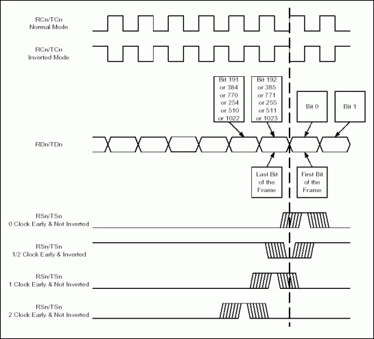
Figure 4. Channelized transmit link timing with normal clock.
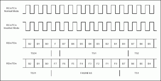
Figure 5. Local channelized transmit link timing with normal clock.
The timing relationship of the receive clock RCn/TCn and data RDn/TDn of a channelized T1/E1 link with normal clock is shown in Figure 4. For a T1 frame, the receive data stream is with a single framing bit (denoted as F) followed by an octet bound to TS1...TS24. The RDn/TDn data bit (B7 of TS1) is clocked in by the first edge of RCn/TDn after the framing bit is the MSB of TS1. The RDn/TDn bit (B0 of TS24) is clocked in by the last edge of RCn before the framing bit is the LSB of TS24. For an E1 frame, the receive data stream is with a single framing byte (denoted as FAS/NFAS) followed by an octet bound to TS1...TS31. The RDn/TDn data bit (B7 of TS1) is clocked in by the first edge of RCn/TCn after the framing byte is the MSB of TS1. The RDn/TDn bit (B0 of TS31) is clocked in by the last edge of RCn/TCn before the framing byte is the LSB of TS31.
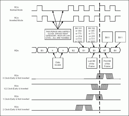
Figure 6. Channelized receive link timing with gapped clock.
The timing relation of the receive clock RCn and data RDn of a channelized link with gapped clock is shown in Figure 6. The receive data is associated with a time slot. Every eight bits are grouped together into a byte with an alignment. The first bit received (B7) is the MSB of an octet. The last bit received (B0) is the LSB. Bits that are to be processed by DS31256 are clocked in on the rising or falling edge of RCn. For gapped clock application, RCn can be held quiescent during any bit of frame. These bits should be ignored (denoted as X). In Figure 6, the quiescent period is shown to be low on RCn. A high level, effected by extending the high phase is equally acceptable. In channelized E1 mode, it must be active continuously at 2.048MHz during all time-slot bits once the frame is not gapped. In channelized T1 mode, it must be active continuously at 1.544MHz during all time-slot bits once the frame is not gapped. In gapped channelized application, RSn must cooperate with the gapped clock. Once there are gapped periods, RSn must extend accordingly. RSn is not an 8kHz synchronization signal.
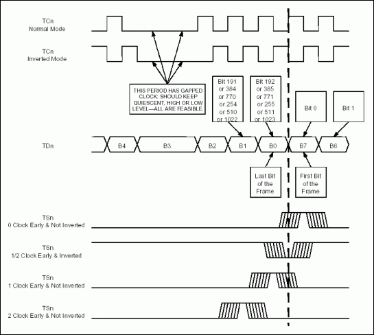
Figure 7. Channelized transmit link timing with gapped clock.
Figure 7 shows the timing relation of the transmit clock TCn and data TDn of a channelized link with gapped clock. The transmitted data is associated with a time slot. Every eight bits are grouped together into a byte with an alignment. The first bit transmitted (B7) is the MSB of an octet. The last bit transmitted (B0) is the least significant bit. Bits that are to be processed by the DS31256 are clocked out on the rising or falling edge of TCn. A transmit link can be stalled by holding the corresponding TCn quiescent. In Figure 7, bit B3 is shown to be stalled for two clock cycles. For gapped clock application, TCn can be held quiescent during any bit of frame. In Figure 6, the quiescent period is shown to be low on TCn. A high level, effected by extending the high phase is equally acceptable. In channelized E1 mode, it must be active continuously at 2.048MHz during all time-slot bits once the frame is not gapped. In channelized T1 mode, it must be active continuously at 1.544MHz during all time-slot bits once the frame is not gapped. In gapped, channelized application, TSn must cooperate with the gapped clock. Once there are gapped periods, TSn must extend accordingly. TSn is not an 8k synchronization signal.
You must configure the corresponding registers for RCn/TCn in normal or inverted mode, RSn/TSn in 0, 1/2, 1, and 2 clock cycles early and inverted or inverted mode. For channelized and unchannelized, gapped or not gapped clock application, you must meet DS31256 AC characteristic demands of layer one ports. Please see the DS31256 data sheet for more detailed information
 電子發(fā)燒友App














評論